


8255
Programmable Peripheral Interface (PPI) / 24 line I/O interface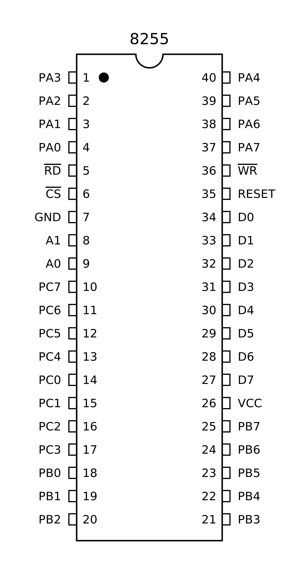
Category: Other | Datasheet
Description
The Intel 8255A (8255) is a general purpose programmable I/O device designed for use with Intel microprocessors. It has 24 1/0 pins which may be individually programmed in 2 groups of 12 and used in 3 major modes of operation. In the first mode (MODE 0), each group of 12 I/O pins may be programmed in sets of 4 to be input or output. In MODE 1, the second mode, each group may be programmed to have 8 lines of input or output. Of the remaining 4 pins, 3 are used for handshaking and interrupt control signals. The third mode of operation (MODE 2) is a bidirectional bus mode which uses 8 lines for a bidirectional bus, and 5 lines, borrowing one from the other group, for handshaking.
Pinout
| Pin | Signal | Dir | Name |
|---|---|---|---|
| 1 | PA3 | Input/Output | Port A bit 3 |
| 2 | PA2 | Input/Output | Port A bit 2 |
| 3 | PA1 | Input/Output | Port A bit 1 |
| 4 | PA0 | Input/Output | Port A bit 0 |
| 5 | RD# | Input | Read Input |
| 6 | CS# | Input | Chip Select |
| 7 | GND | Power | Ground |
| 8 | A1 | Input | Port Address 1 |
| 9 | A0 | Input | Port Address 0 |
| 10 | PC7 | Input/Output | Port C bit 7 |
| 11 | PC6 | Input/Output | Port C bit 6 |
| 12 | PC5 | Input/Output | Port C bit 5 |
| 13 | PC4 | Input/Output | Port C bit 4 |
| 14 | PC0 | Input/Output | Port C bit 0 |
| 15 | PC1 | Input/Output | Port C bit 1 |
| 16 | PC2 | Input/Output | Port C bit 2 |
| 17 | PC3 | Input/Output | Port C bit 3 |
| 18 | PB0 | Input/Output | Port B bit 0 |
| 19 | PB1 | Input/Output | Port B bit 1 |
| 20 | PB2 | Input/Output | Port B bit 2 |
| 21 | PB3 | Input/Output | Port B bit 3 |
| 22 | PB4 | Input/Output | Port B bit 4 |
| 23 | PB5 | Input/Output | Port B bit 5 |
| 24 | PB6 | Input/Output | Port B bit 6 |
| 25 | PB7 | Input/Output | Port B bit 7 |
| 26 | VCC | Power | Power supply (+5V) |
| 27 | D7 | Input/Output | Data Bus bit 7 |
| 28 | D6 | Input/Output | Data Bus bit 6 |
| 29 | D5 | Input/Output | Data Bus bit 5 |
| 30 | D4 | Input/Output | Data Bus bit 4 |
| 31 | D3 | Input/Output | Data Bus bit 3 |
| 32 | D2 | Input/Output | Data Bus bit 2 |
| 33 | D1 | Input/Output | Data Bus bit 1 |
| 34 | D0 | Input/Output | Data Bus bit 0 |
| 35 | RESET | Input | Reset Input |
| 36 | WR# | Input | Write Input |
| 37 | PA7 | Input/Output | Port A bit 7 |
| 38 | PA6 | Input/Output | Port A bit 6 |
| 39 | PA5 | Input/Output | Port A bit 5 |
| 40 | PA4 | Input/Output | Port A bit 4 |
Registers
| Addr | A0 | A1 | Register |
|---|---|---|---|
| 0 | 0 | 0 | Port A |
| 1 | 1 | 0 | Port B |
| 2 | 0 | 1 | Port C |
| 3 | 1 | 1 | Control |
If you notice any errors in the database, please let me know!