M8SBC-486: Soldering and testing first board
[Go back to the main page of this project] [Previous part]

Soldering
The PCBs arrived a week after I placed the order (so production and shipment only took a week!). After they arrived, I immediately started soldering them since I already had all the parts.
Just to note, I was working on the chipset as I was working on the board. The previous part is more about the final result of the chipset. Some parts were not yet implemented at the time this story was taking place.
First, I soldered all the small SMD parts, such as resistors and capacitors. Then, I worked on the power section (2.5 V and 3.3 V regulators) to make sure there were no shorts. Fortunately, there were no shorts and the correct voltages were present on all rails. Since the board was still empty, I decided to work first on the parts that required a lot of precision. This meant soldering the 144-pin QFP FPGA next. I could also test it afterwards.
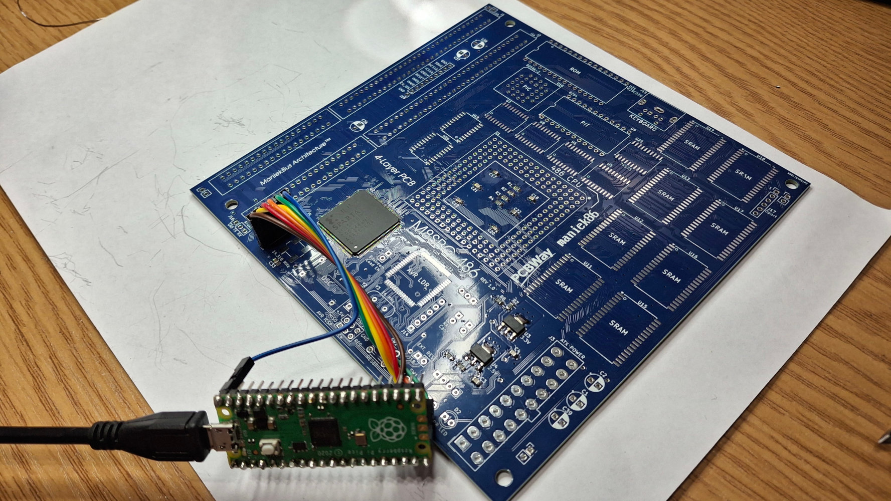
I connected my Raspberry Pi Pico-based Xilinx virtual cable, and the XC2S100 was detected in the Xilinx iMPACT software. Good! For those wondering how I used the Raspberry Pi Pico as a JTAG cable, I used a project named xvc-pico, which turns the Pico into a Xilinx Virtual Cable. The Xilinx Virtual Cable protocol lets you use programmers over TCP/IP. Since this protocol is well documented, it can also be used locally to connect Xilinx iMPACT to 3rd party projects, which can emulate a cable like this. The last version of Xilinx ISE (an old IDE for programming Xilinx FPGAs) to support the Spartan II FPGA family is Xilinx ISE 10.1, released in 2008. These FPGAs were released around 1999! The iMPACT programming tool in this version doesn't support the XVC protocol so, to make the xvc-pico project work, I used Xilinx iMPACT from ISE 14.7, which still supports Spartan II even though its IDE doesn't.
Anyway, as you may remember from the first part, FPGAs don't store their configuration. So, this is useful for debugging and verifying that the chip is working. Next, I soldered the ATMega128, which has flash memory and will act as the bitstream loader for the FPGA. Then, I soldered the rest of the SMD chips such as the 74 logic ICs and SRAMs. While soldering the SRAMs, I noticed something unusual about them - almost every SRAM had a different pin one marking. I ordered them cheaply from AliExpress, so I could have expected something sketchy about them. I don't really mind relabeled chips as long as they function properly. I haven't had any issues with cheap chips from AliExpress before. So, after soldering the SRAM, I powered the board in order to test it and I found out that there was a short. The issue was one SRAM chip. After closer inspection, I saw that the label was printed upside down which caused me to solder it in reverse. Since I had a pack of ten, I replaced it with another one and the short was gone. I decided to check one remaining SRAM chip in my XGecu T48 programmer (they have the ability to check some memory chips) by making a crude SOP to DIP adapter and for my luck, it worked fine.
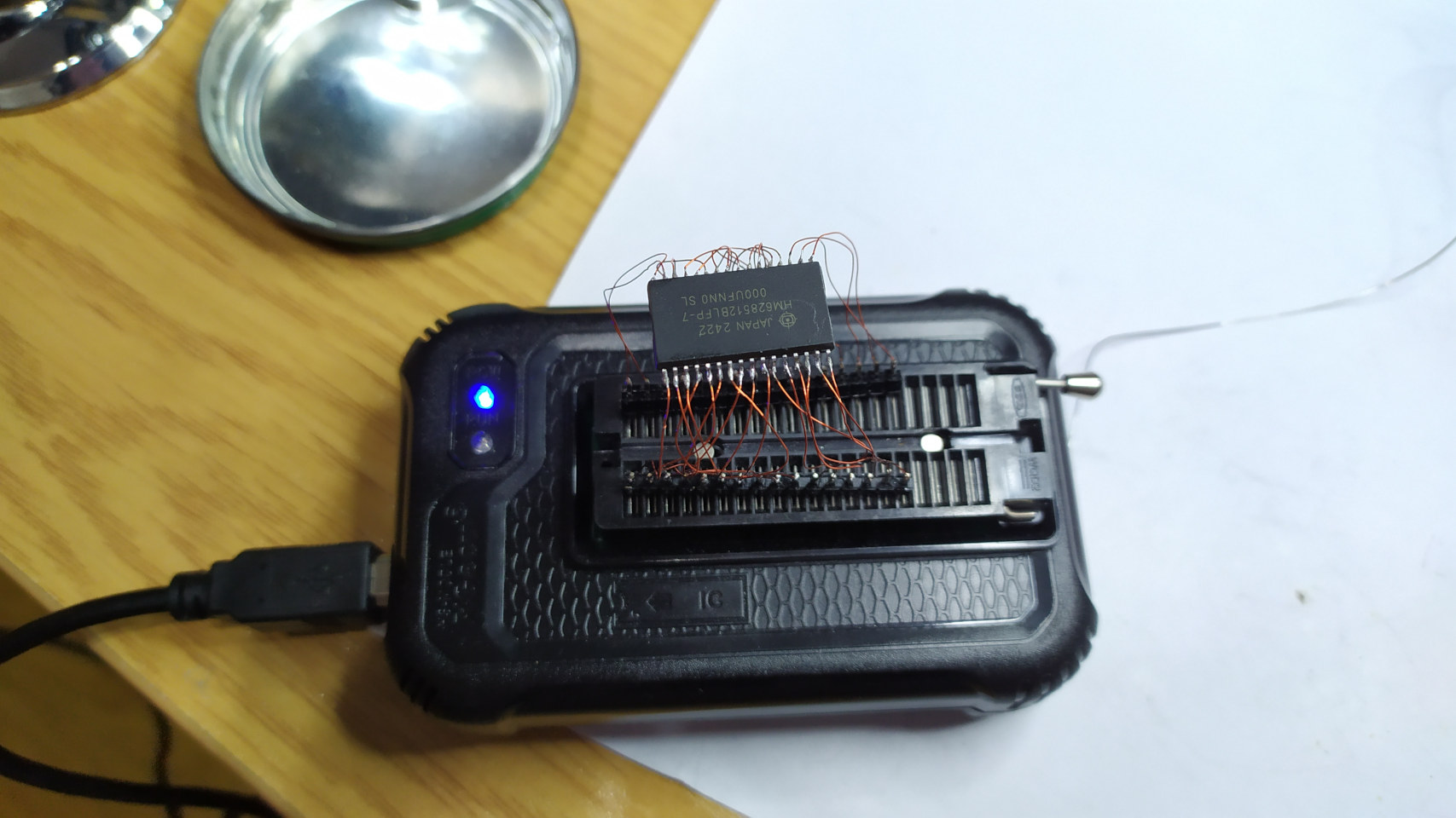
This one had the label printed upside down too!
After soldering all the SMD parts, such as resistors, capacitors, and chips, as well as the unmentioned 14.138 MHz SMD oscillator, I moved on to the THT parts, sockets, and connectors. Soldering oscillators, pin headers and DIP sockets was not difficult, but soldering - or rather, making - the PGA socket was challenging! PGA sockets, especially for retro CPUs (like the 486, which uses PGA-169, but one pin is unused, so it's really PGA-168), are hard to find and ZIF ones are even harder! I actually had a lot of precision DIP sockets that I bought for the ROM IC. I came up with the idea to cut them precisely and make an LIF PGA socket out of them. After an hour of work, I managed to make something out of them. I had to cut them a little bit because they didn't want to go one after the other, but after that, they fit perfectly.
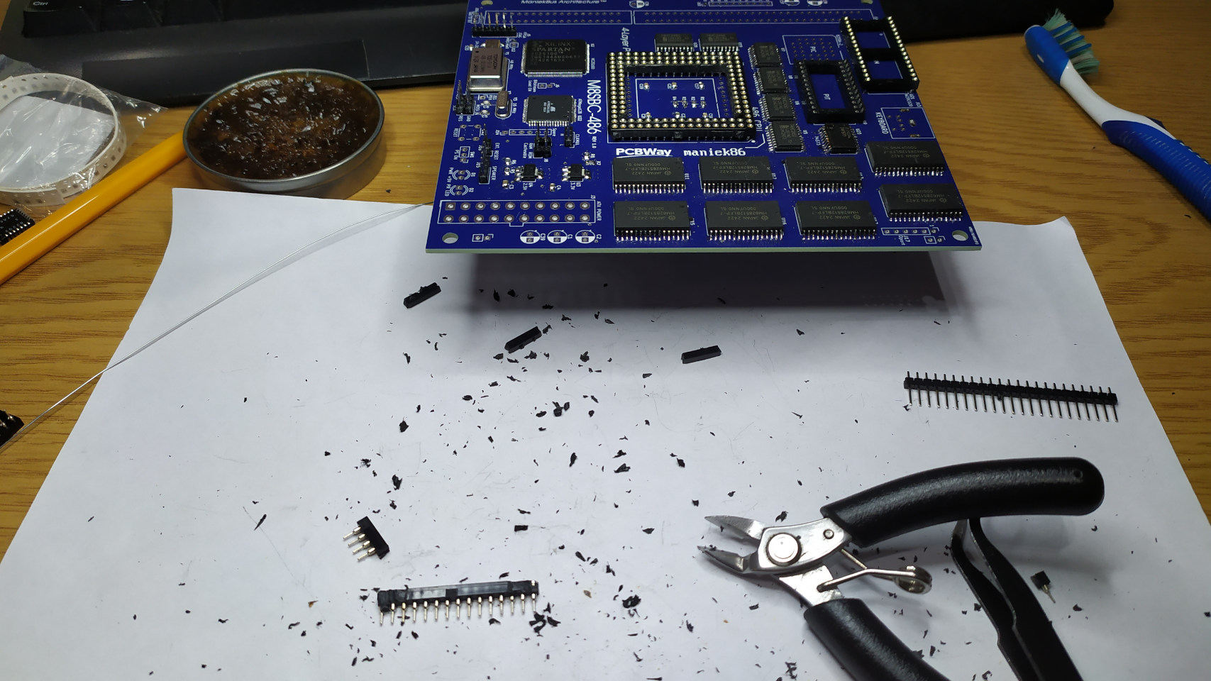
Such a mess!
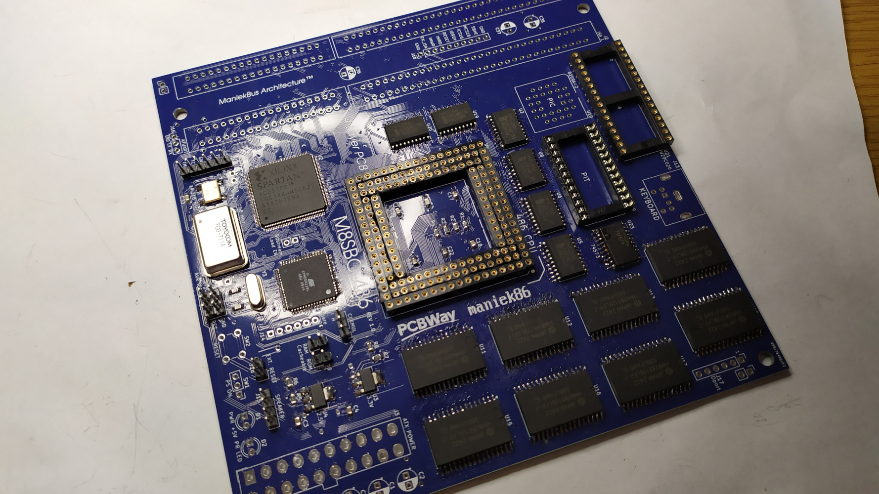
I bought only one 16-bit ISA slot for the board because these are kinda expensive, so the board initially had only one ISA slot. This later changed when I decided to "borrow" an ISA slot from one of my boards from my collection - from a crappy Socket 370 board (this happened few days later, so that's why the next images of the PCB will still have one ISA slot). And in the end, I soldered a few missing jumpers, electrolytic capacitors, a keyboard connector and a 20-pin ATX power connector that I had harvested a long time ago from a dead motherboard.
It works!
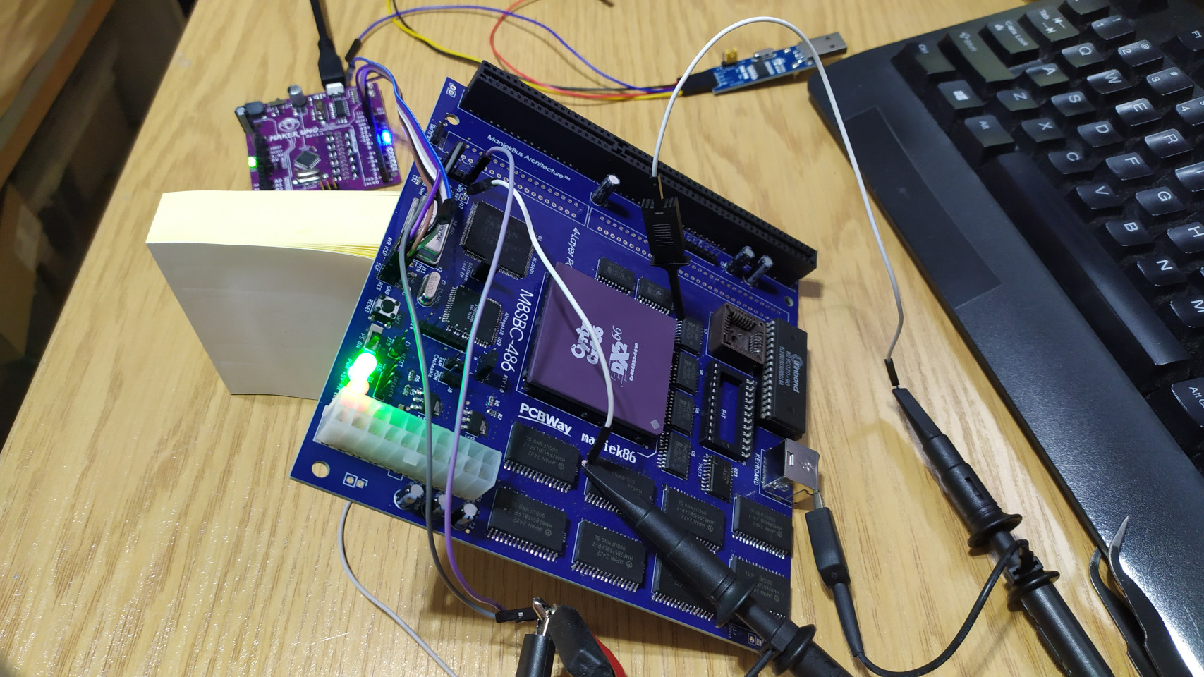
I finished soldering the board on Thursday and I spent my entire Friday afternoon until almost 3 a.m. working on it! I already had the ATMega128 bitstream loader working, so the task was to fix a few things in the chipset code and get a simple infinite loop to work. After a lot of tinkering and with the help of my oscilloscope, I got it running. I can't describe how happy I was to see the 486 execute an infinite loop on my custom board! This meant that many crucial things were done right, both on the PCB and in the chipset. Just imagine: To make the 486 access the 8-bit ROM (and execute code from it), the bus transceivers must be functional to swap data on the 32-bit bus. The A0 and A1 must be decoded. The address decoder must work. Read signals must be generated. And, since I was testing at 12 MHz, a state machine must be made to generate wait states for slower ROM. Amazing!
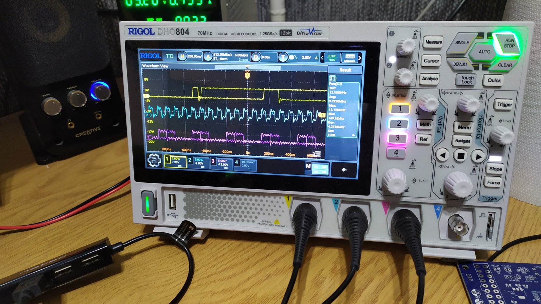
As far as I can remember, signals from the top are: some data line, CPU clock and ROM read signal.
The next day, I noticed one mistake. It wasn't fatal, but for a few moments I felt like I had messed up a lot. The problem was that for some reason, the PCB footprints for the 8259 PIC and the 8254 PIT had been swapped. Looking at my parts and the PCB design, I realized there were no DRC errors about incorrect connections when I ordered the PCB. I looked it up online and found that both of these ICs come in DIP and PLCC packages, but I had ordered them backwards. The 8259 PIC that was supposed to be in PLCC was in DIP, and the 8254 timer that was supposed to be in DIP was in PLCC. Duh! I decided to just order the correct parts again from AliExpress. This delayed the implementation of these parts a bit, but at least I could work on other things, like ISA in the meantime. Also, there were holidays in China, so I waited a few more days for the chips.
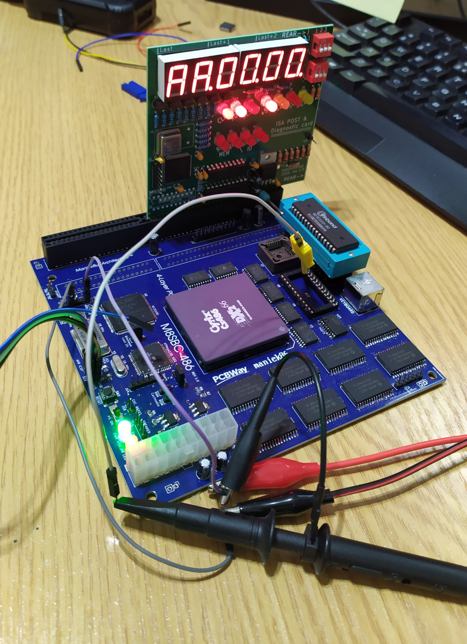
For the time being, I started working on the ISA bus. As I mentioned in the previous part, the 8-bit ISA is simple, so implementing basic 8-bit transfers didn't take too long. Below is a picture of my open source POST card working with my open source motherboard!
ISA VGA
At the time, I only owned two 16-bit ISA SVGA graphics cards. One was a Trident TVGA8900C and the other was a Cirrus Logic GD5428. The GD5428 is a 16-bit ISA-only card (which I later found out to be untrue after experimenting) and the TVGA8900C uses 16-bit ISA but can work in both 8 and 16-bit ISA slots. I chose to use the Trident card. For my previous homebrew project, I had initialized this card using a decompiled video BIOS from GitHub. However this time, I wanted to use the VGA BIOS ROM. After doing a lot of internet research, I found out how to do it. The VGA BIOS ROM is usually located at the 0xC0000 memory location on the ISA bus. All we have to do is call it and it should do everything for us and return. First though, we should check if the VGA ROM (or in general, the graphics card) is present on the bus. This can be done by checking the first two bytes of that ROM. They should be 0x55 0xAA. Furthermore, The third byte is the size of the ROM divided by 512. Finally, the fourth byte is the entry point. It's usually a JMP instruction. As execution ends, RET is called and we can resume our main execution. The graphics card should get initialized and hook up its real mode routines to int 10h.
I already had the C language running in real mode, so coding this was not difficult. The only difficulty I had was calling the VGA ROM BIOS and later returning normally to the C code. However, I encountered a problem where the CPU would crash during execution of the ROM code. I started decompiling a dump of the VGA BIOS from that card to see what was happening, and I noticed INT 10H calls. Why would the graphics card try to call a routine that it should hook up? I think it's because of how earlier video cards worked, like the CGA and MDA. In both of these standards, the BIOS initialized them. There were no option ROMs that took care of initialization. The VGA BIOS probably checks for that. To fix the issue, I created a stub int 10h handler that gets hooked up before calling the VGA BIOS, and it worked!
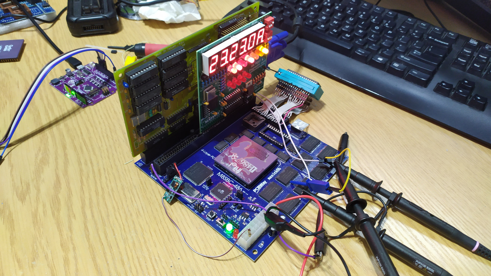
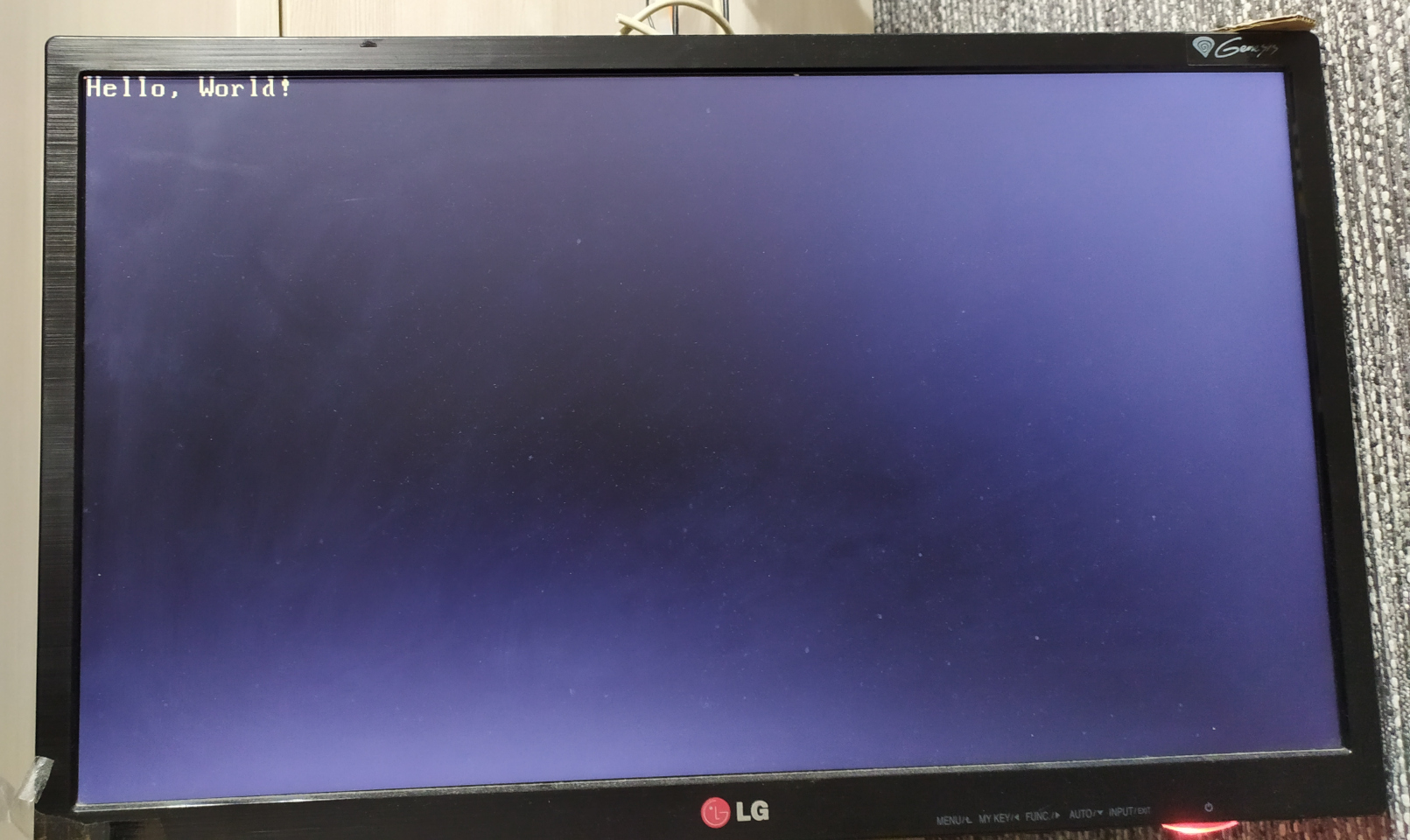
The card initialized in 03h video mode, which is a 16-color 80x25 text mode. I could use INT 10H routines to print to the screen, as well as use direct memory access at 0xB8000. At this point, I began developing my BIOS. (Read more about it in the next part. Here, I will just continue with the hardware)
Missing PIC issue
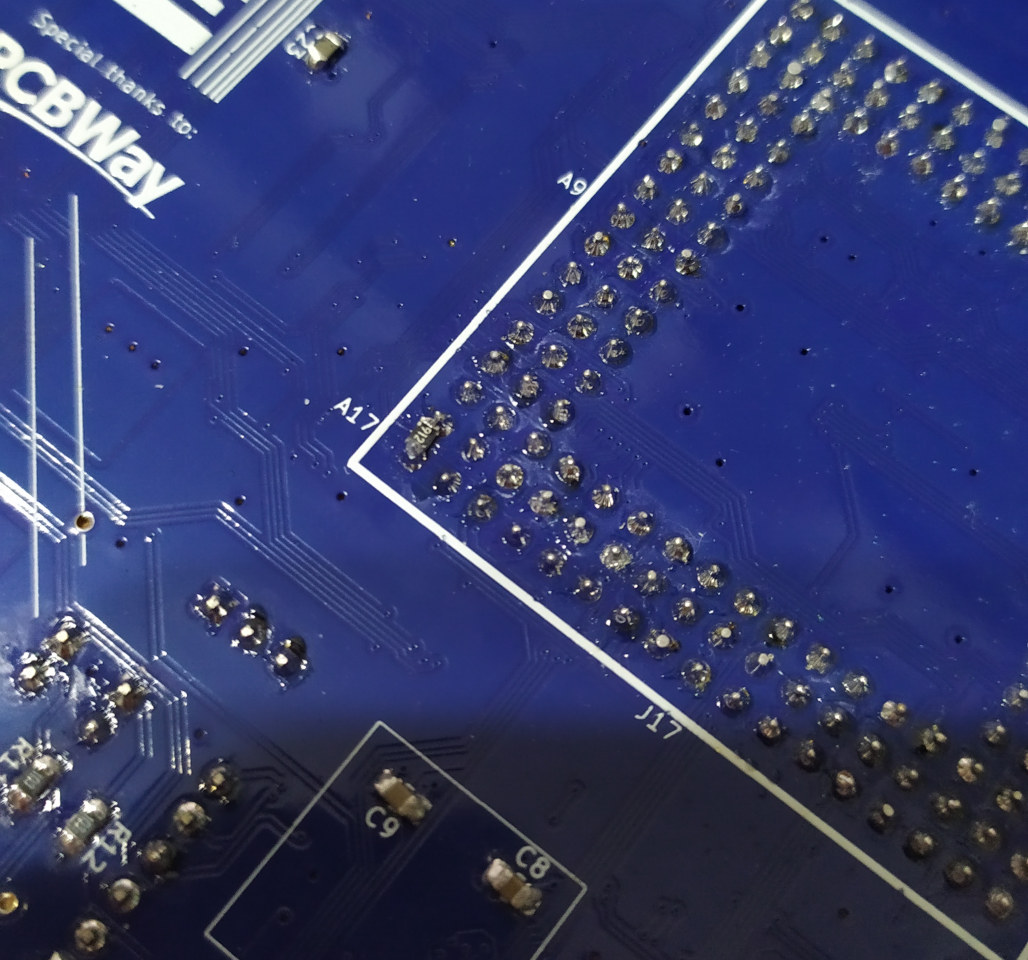
As I progressed, I noticed some strange behavior. Sometimes, the VGA BIOS would not initialize after powering up. To make it work, I had to power it up, wait for it to freeze, and then reset it using the button. It was strange because touching some CPU pins changed the behavior (e.g., the crash would occur at a different time than VGA initialization). At first, I suspected the chipset design but after examining the PCB design for some time, I noticed that the processor IRQ line was floating. During the design process, I hadn't considered a situation in which the interrupt controller was absent (I was still waiting for it to arrive). Looking at the socket pinout, I noticed that the IRQ line was right next to the GND pin. I decided to add a hack resistor to pull it to ground. The issue was gone!
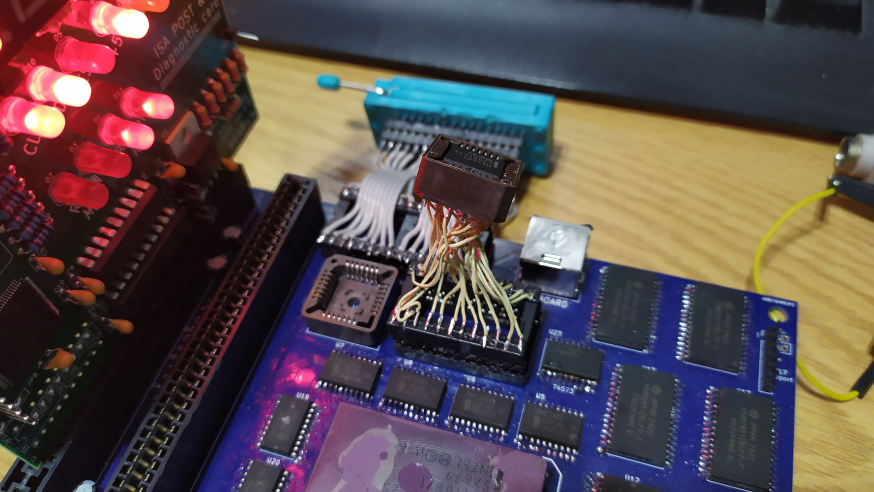
DIY PLCC to DIP adapter
I was impatient waiting for the PIC and PIT. Looking at the parts I had mistakenly ordered, I realized that I could try adapting the PIT in the PLCC package to the DIP, as I still had some PLCC sockets left. So, I did. The result looked ridiculous, but it worked!
Meanwhile, I tested various CPUs. All of the major 486 CPUs worked: Intel (including SX, DX, and DX2), AMD, and Cyrix. In a previous 486 homebrew project on a prototype board, I could not get the Intel 486 to work. I guess the Intel 486 is stricter about timings and interference. I would like to thank tomekmak.xoc and KacperL for donating the hardware (including the 486 CPUs), which helped me test this board further!
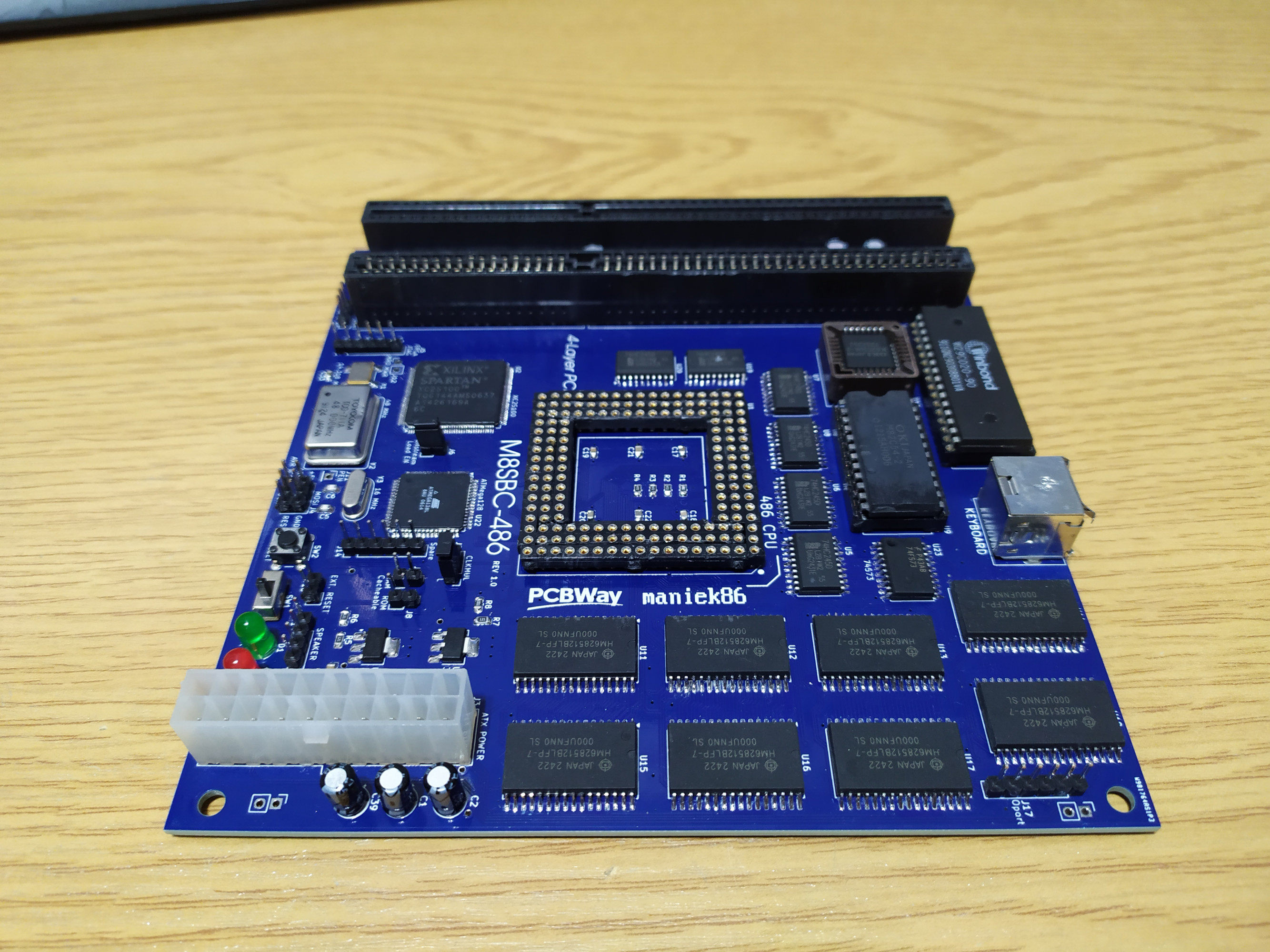
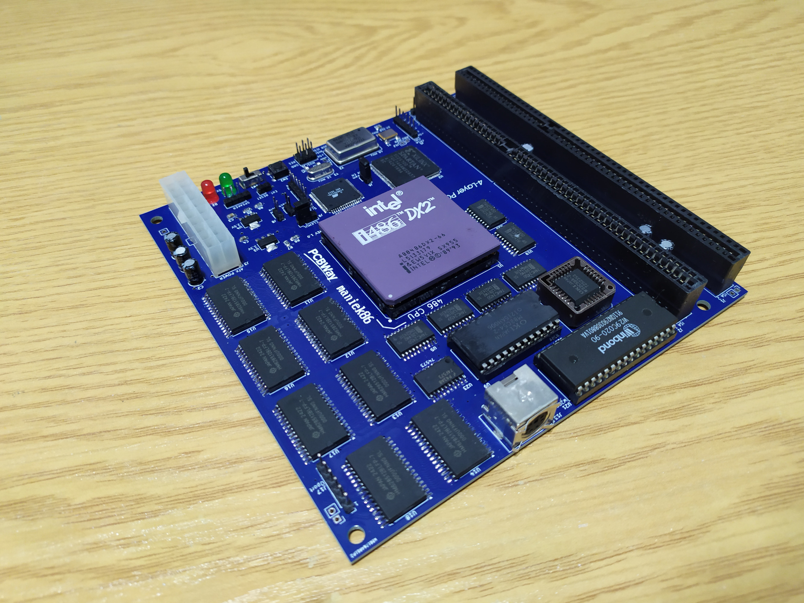
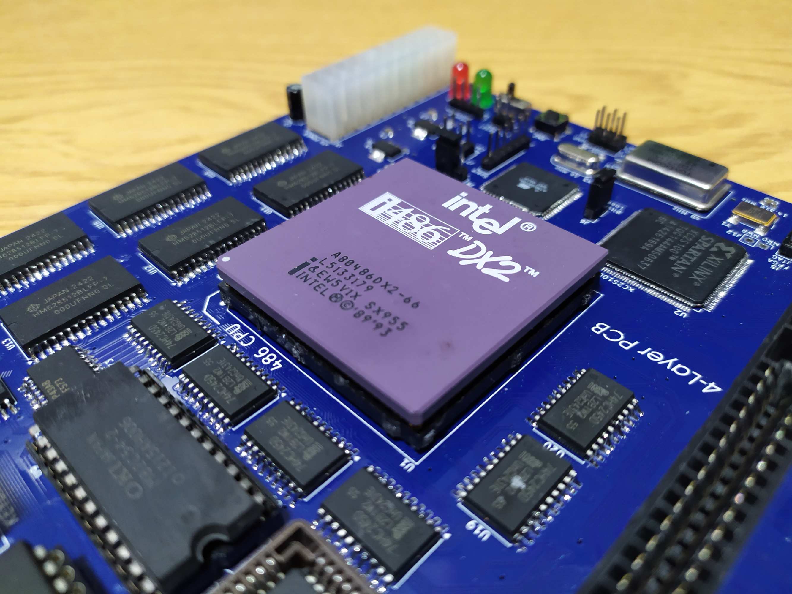
Finished result
Once the correct PIT and PIC arrived, I added support to the interrupt controller in the chipset. I had to implement interrupt acknowledge generation. The 486 interrupt acknowledge is pretty much compatible with the classic 8259 PIC, except that we have to decode the signal from the control signals. I thought it would be difficult to use interrupts, but after experimenting with them, I realized they aren't so complicated. In the end, I gave the entire board a bath in isopropyl alcohol, and it was pretty much done!
Last updated: 09/01/2026


![Validate my RSS feed [Valid RSS]](http://maniek86.xyz/cmsesus/uploads/image/valid-rss-rogers.png)
