Homebrew 68000 computer
[Back to the homebrew computers page]
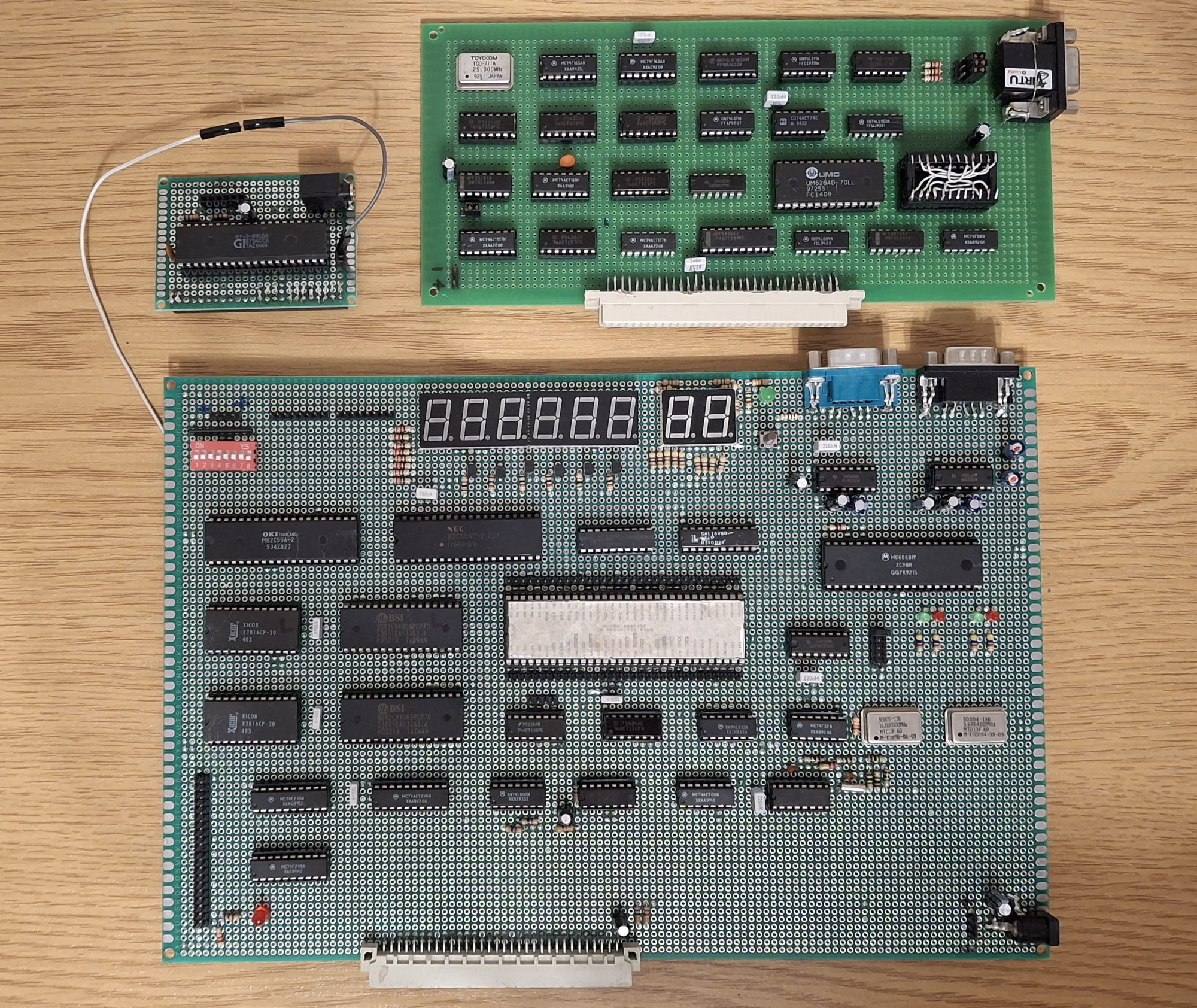
The finished result
Specs
- Motorola 68000 running at 16 MHz
- 1MB of SRAM
- 4KB of ROM
- Two Intel 8255 - total 48 I/O lines
- 2 Serial ports
- IDE interface
- One expansion port
- 2048Hz clock for timing
Current state: Lying in my closet, still working and ready to go
Repository with various stuff made during development: https://github.com/maniekx86/homebrews_m68k
Schematic: http://maniek86.xyz/pliki2/projekt_m68k/m68k.pdf
Graphics card schematic: http://maniek86.xyz/pliki2/projekt_m68k/vga_gpu.pdf
History
Parts gathering
It was May of 2024, just a few months after I had stopped working on the 6502 homebrew project. Out of curiosity, I was browsing the Polish auction site Allegro Lokalnie and found an interesting offer: 10 kg of electronic scrap up for auction. I noticed it wasn't boring scrap. In fact, I saw hundreds of ICs! From the seller's low quality photos, I could see that these were mostly logic gates but there were also larger ICs. It was some kind of mainframe! I also spotted that the gold edge connectors had been cut, probably by the previous scrapper. One large IC in a standard 2.54 mm DIP package caught my attention. After doing some research, I found out that it was a Motorola 68000. I decided to bid on it. At this point, I wasn't particularly interested in the CPU but you'll see that change later.
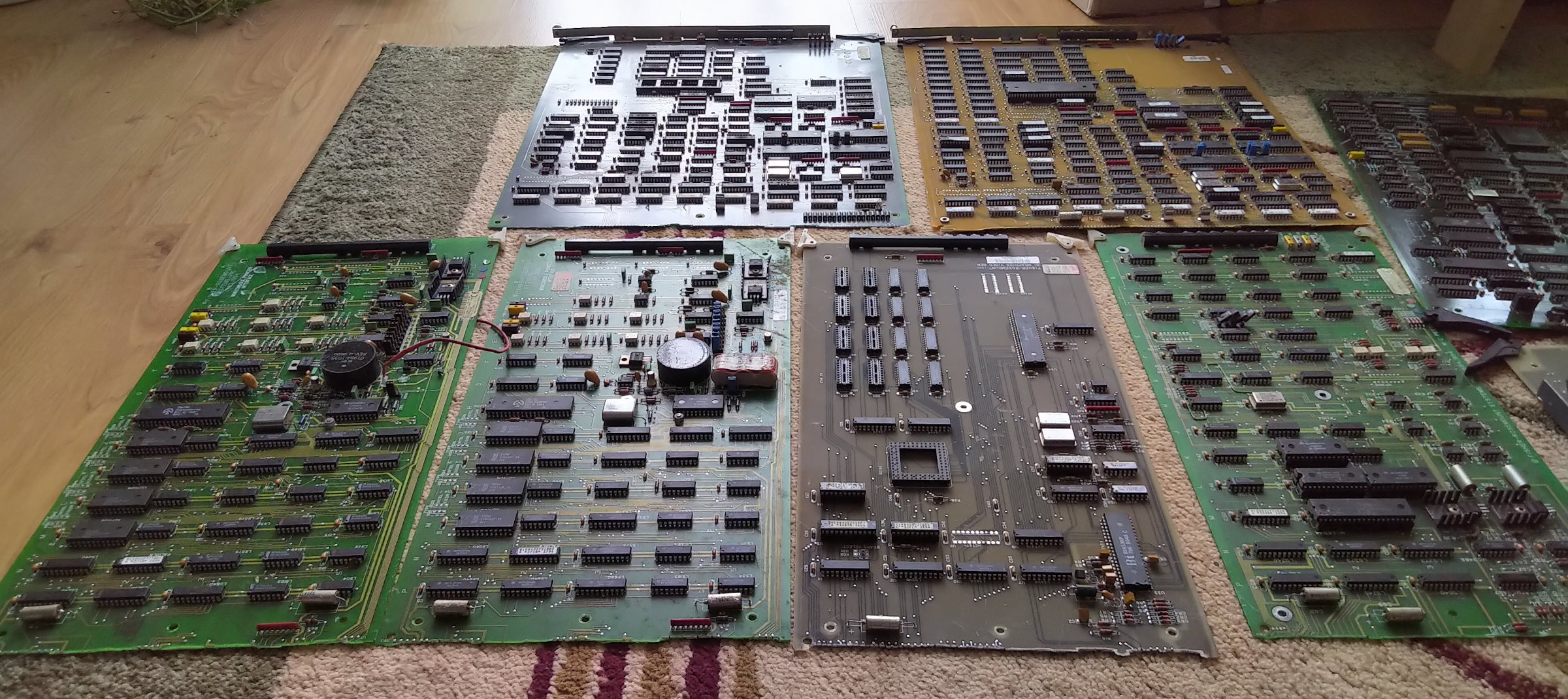
In the end, I was bidding against one other person, but they gave up at 110 PLN, so I won the scrap for that price. 110 PLN is about $30 (2025) and delivery was free. The scrap arrived a few days later and it looked very promising! I gave it a quick bath in water before desoldering everything with a hot air gun. I made sure the boards were dry before doing that (I left them to dry for a few days). There was no point in getting it running again. Not only were the edge connectors cut, but many socketed ICs were also missing. Below is an image of the scrap when it arrived.
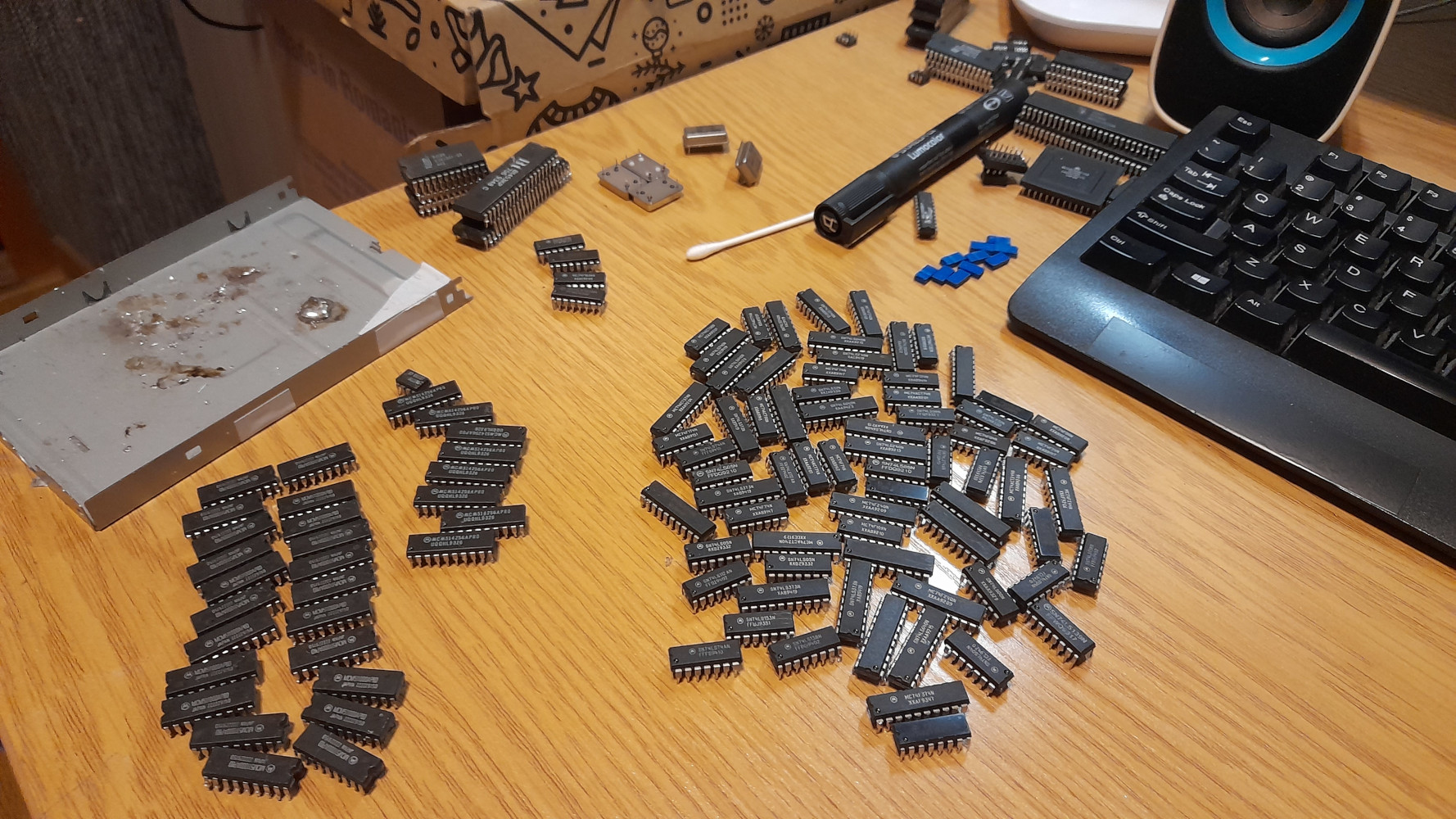
After desoldering, I tested almost every chip in my recently acquired XGecu T48 programmer. It has a feature that checks logic chips. I don't recall any being faulty.
Meanwhile I've started reading about Motorola 68000 and it drawn more attention to me. Most interesting thing about it was that it was in the 2.54 mm DIP package and I could plug it into breadboard. Also the fact of it being 16-bit instead of 8-bit. So finally after a lot of considerations I decided to start experimenting with it.
Motorola 68000 homebrew on a breadboard
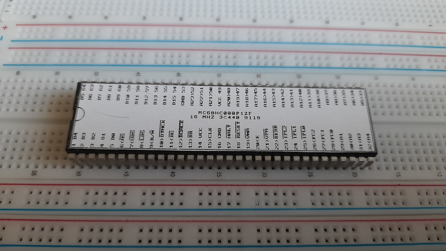
To do that, I bought six breadboards. I put them together to make a large 2x3 breadboard. Since I had access to a label printer, I decided to print a nice sticker with a description of the pins of the Motorola 68000. This made working on the project easier, since the Motorola 68000 is in a large DIP-64 package.
The next day, I got to work. At the time, I had two 512 KB SRAM chips - BS62LV4008PCP70 from another scrap. Since two 8-bit chips are perfect for a 16-bit CPU, I used them for RAM. The Motorola 68000 has 24 address lines and can therefore address a maximum of 16 MB of memory. With these two chips, I have a total of 1 MB of RAM. That's plenty for a breadboard computer. However, the ROM is a different story. At that moment, I couldn't find any suitable EEPROMs or flash chips. I wanted two chips like the RAM so that I wouldn't have to create logic to translate the 8-bit ROM to the 16-bit CPU bus. Ultimately, I decided to use small 2 KB EEPROMs that I found in the same scrap pile (there were plenty of 2 KB 2816 EEPROM ICs in it). I thought, Since I have a lot of RAM, I could write a small bootloader and load programs from the serial port or hard drive into the RAM.
Through some experimentation, trial and error, by reading datasheets and looking up references on the Internet, I managed to get the CPU to execute something the same day. Again, it was just an infinite loop at first but the result was satisfying.
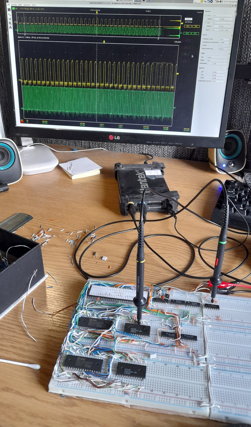
To generate the clock this time, I used a Schmitt inverter and a 4.5 MHz crystal resonator. Initially, I added a 74161 binary counter to divide the frequency as it's easier to debug with a lower clock. I used the remaining gates of the Schmitt inverter, two 7432 OR gates and one 7408 AND gate for the glue logic. This time, I also went without a schematic but the connections are similar to the final result of this project, so you can check the schematic of the prototype PCB version. The address decoder was made on a 74138 again. It divided memory perfectly into 1 MB chunks. For example, connecting RAM CS lines didn't require anything more.
One detail worth noting in my design is that the DTACK signal of the Motorola is grounded. The DTACK signal basically indicates whether the external device on the CPU bus has finished writing or reading. It's similar to the RDY signal on 6502 and x86 chips.
The next thing I added was the 8255 I/O. You may also notice the 8255 in my earlier and later projects. This is because I bought a bunch of them on AliExpress when I was working on the homebrew 6502 computer (I had one from scrap and later bought five of them). To generate Intel's WR and RD signals from the Motorola 68000 signaling, I had to add a 7400 NAND gate. Below is a video of a simple LED blink and the most complicated LED switch. By "most complicated" I mean that I added a DIP switch connected to the I/O pins. The LED was enabled when any of the eight DIP switches were on. Therefore, the CPU must read and write from the I/O chip.
You might be wondering how I programmed this thing. The Motorola 68000 is a powerful processor and GCC has been ported to it. This means that we can program it in modern C. However, at the beginning, I decided to use assembly because it's the closest to the hardware. The blink program looked like this:
.ORG $810000
START:
    JSR     DELAY ; wait a bit
    ; Initialize 8255
    MOVE.B  #$80, D0         ; D0 = 0b10000000
    MOVE.B  D0, $100006      ; Register 3; Addressing is multipled by 2 because 8255 A0 is connected to the A1 and so on (Motorola 68000 doesn't have A0)

BLINK:
    ; Turn the LED on (set all PA pins high)
    MOVE.B  #$FF, D0         ; D0 = 0xFF
    MOVE.B  D0, $100000      ; Write to Port A ($100000)
    JSR     DELAY            ; Call delay subroutine

    ; Turn the LED off (set all PA pins low)
    MOVE.B  #$00, D0         ; D0 = 0x00
    MOVE.B  D0, $100000      ; Write to Port A
    JSR     DELAY            ; Call delay subroutine

    BRA     BLINK            ; Repeat the loop

DELAY:
    ; Simple delay loop
    MOVE.L  #40000, D1      ; Delay count
DELAY_LOOP:
    SUBQ.L  #1, D1           ; Decrement the delay counter
    BNE     DELAY_LOOP       ; If not zero, continue the loop
    RTS                      ; Return from subroutine
I don't remember the exact peripheral addressing on the breadboard version, but we can see that the 8255 was present at address 0x100000.
With my first programs, I started to really like the Motorola 68000 assembly. It has sixteen full 32-bit registers. Eight are used for data and eight are used for addressing. Next are the instructions. Instructions can operate on a byte, a word or a long word. This can be specified by adding .B, .W or .L after the instruction. It's just very enjoyable!
To compile and build this assembly code at the beginning, I found on the internet a ASMX cross assembler which can compile assembly for the 68000 and run on modern Linux. I had to use a hex editor to manually assemble the image to make it compatible. I had to place the binary at the correct place, insert the entry vector at the beginning and use a C program to split the ROM into odd and even bytes at the end.
Later on, I also wrote a simple memory test to check if the memory was working. I kept it on separate EEPROMs for quick access because I had many problems with signaling. I used poor quality wires from Ethernet cable that caused the computer to crash or fail to boot again after slight contact with the wires or vibration (for example, when bumping my desk with my leg). The problem was mainly caused by the RAM connected by these wires on the left, as you can see in the photos.
My next step was to implement the IDE controller. I didn't have much ROM, so in order to run larger programs, I needed to load them into the larger RAM (as I mentioned before). To adapt the 40-pin IDE, I built a DIY breakout board that exposed the most important IDE signals to the breadboard. Since the Motorola 68000 has a 16-bit memory interface and the IDE is also 16-bit, the interface consists only of transceivers that buffer the data, address and control signals. I already had the Intel style WR and RD signals from the 7400 NAND gate which was also used for the 8255 IC. Making it was just a matter of connecting a lot of wires. Image below.
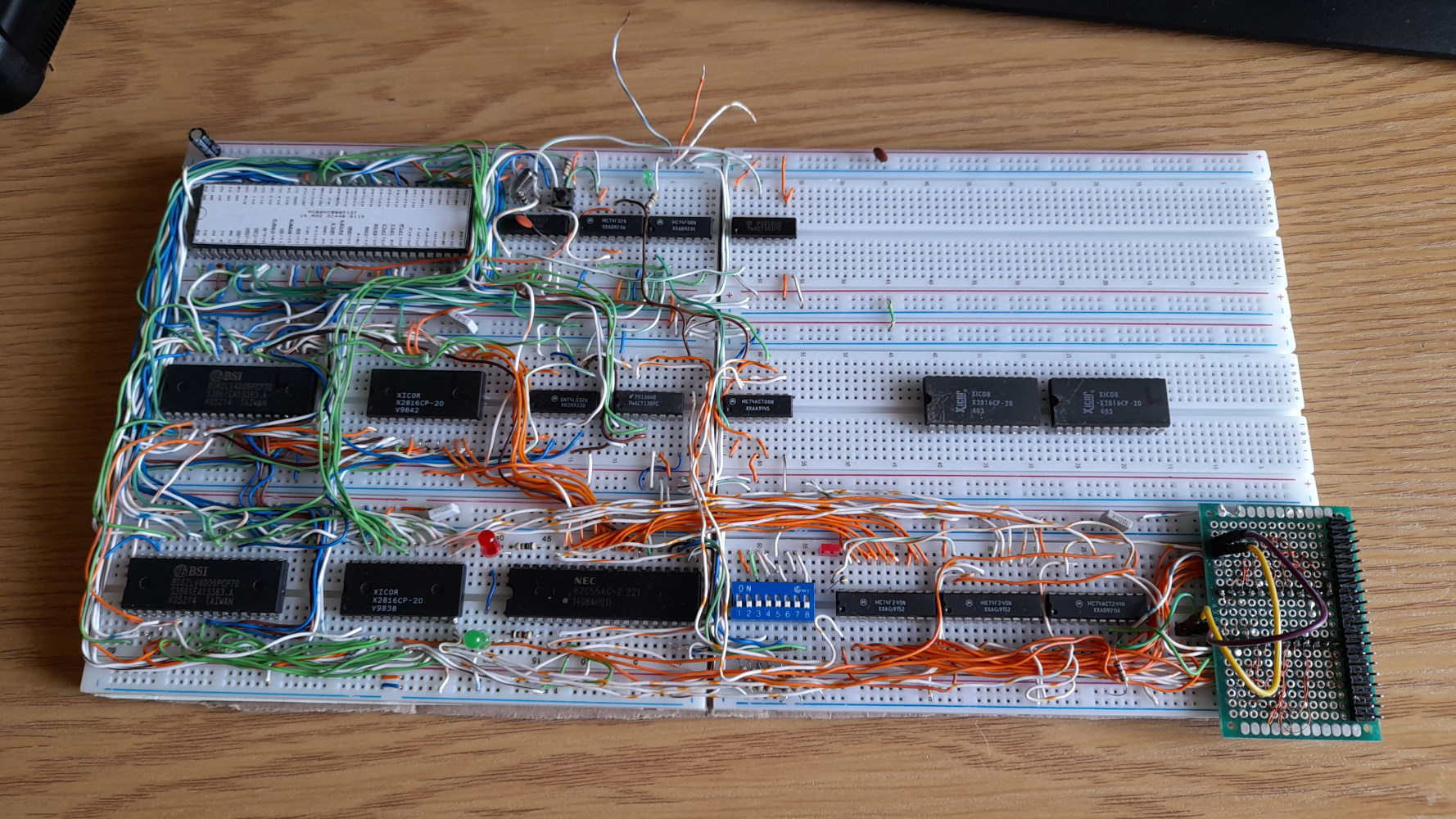
At this point, I've started to write the bootloader. I made it just a "simple" FAT16 bootloader that searches for the BOOT.BIN file, loads it into memory and jumps to it. To be honest, it wasn't an easy task. For someone writing a bootloader for the first time, especially in assembly it was not easy. I used a logic analyzer connected to the 8255 I/O to output debug codes. I tested constantly on the physical machine because I didn't have an emulator. But honestly, as I mentioned before, the Motorola 68000 assembly is pretty nice. I mentioned the data length prefixes (.B, .W and .L) - by using the same instructions with different prefixes, I could perform operations on integers of various sizes. This is fundamental for a FAT driver, as we need to calculate data positions based on headers and the FAT table. The source code is available on the project's GitHub.
Using only an 8255 I/O chip for the human interface is boring. I need a UART. I haven't worked with this type of chip before because I didn't have one when I was working on the 6502 computer. Fortunately, this time I got a Motorola 68681 from the same scrap. It's a dual UART chip. It's designed to operate with 68xxx CPUs, which is great. I checked the datasheet and connected it to my computer.

It also needs to be clocked at 3.6864 MHz. In the scrap there was a clock oscillator dedicated to that, so I used it.
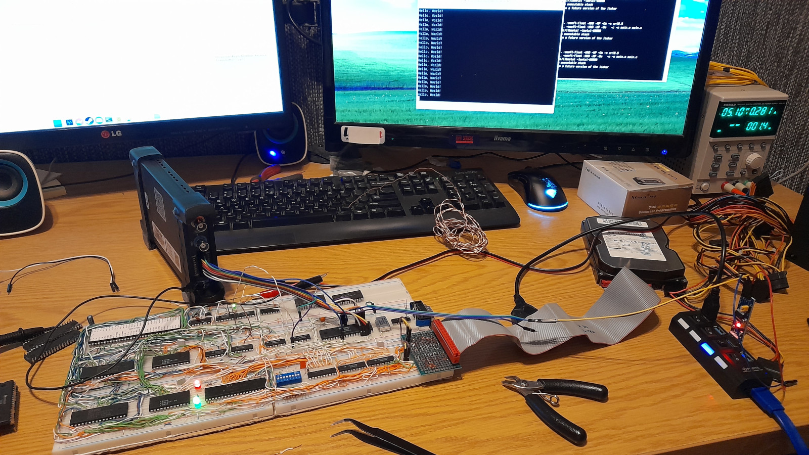
Homebrew 68000 computer - final design
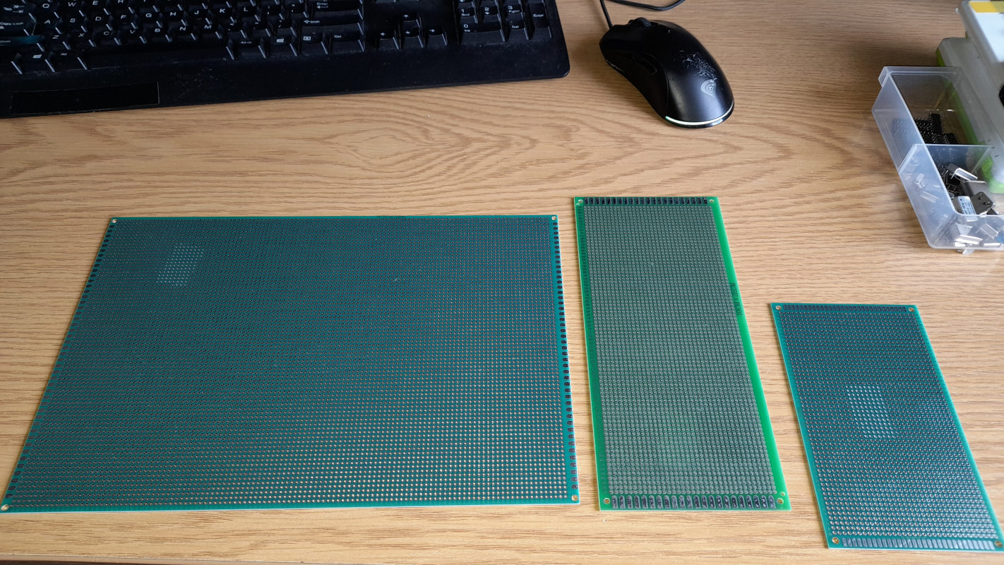
At that time, I had saved up some pocket money, so I finally decided to move this homebrew computer onto something more robust: a prototype PCB. I bought a large, 30*20 cm prototype PCB for the base.
Finally, before soldering it, this time I decided to make a schematic. After all, there are a lot more connections here. I created it in KiCad based on my research from the breadboard version. The schematic and specs are available at the top of this page as they're final. Making the schematic took me about two days. I printed the schematic on paper and marked with a pencil which connections were complete. While soldering, I found an issue where I had connected the NAND gate incorrectly. The schematic on this page has already been fixed, but I just fixed the paper copy manually. The prototype PCB version also included a CPU frequency selection jumper. I used a 16 MHz crystal clock and a 74161 binary counter IC to divide the clock to 8, 4, 2 and 1 MHz.
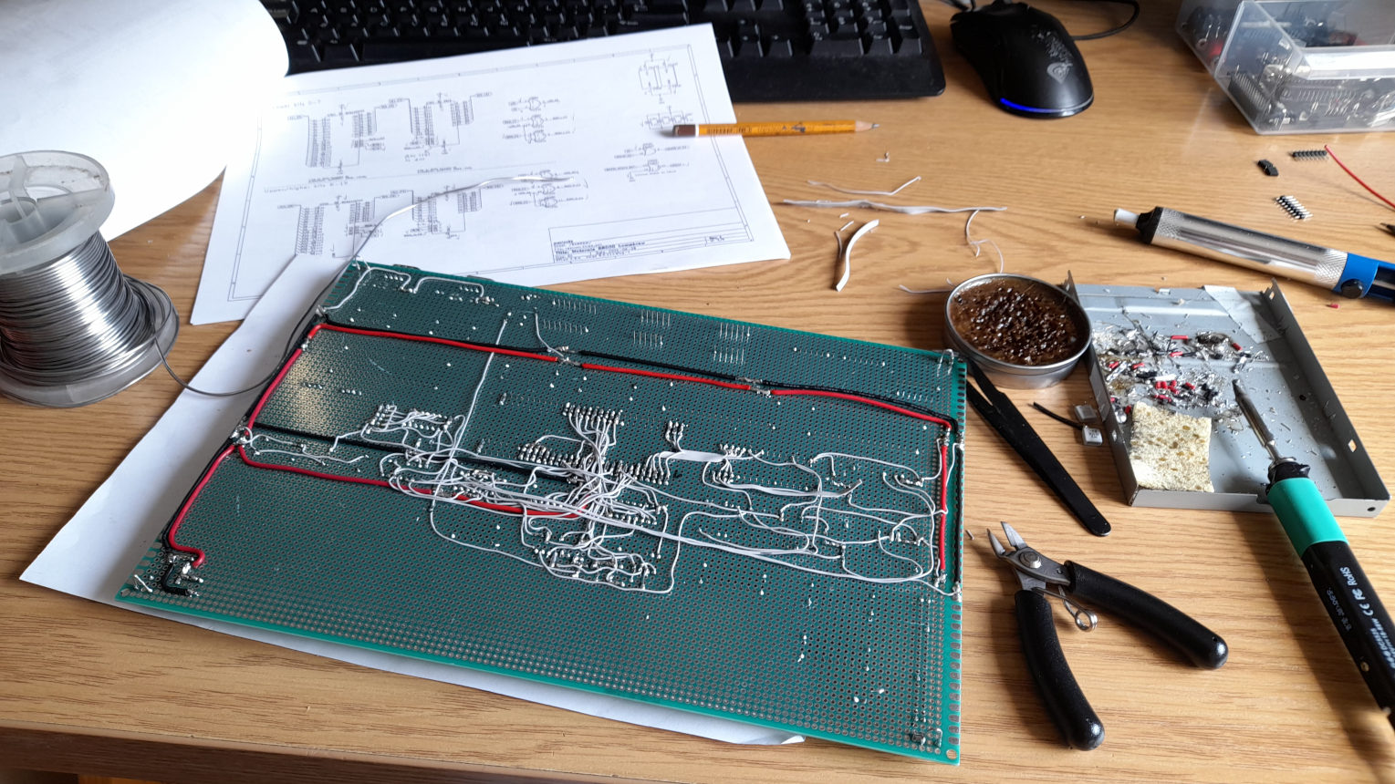
Above is video showing first tests of prototype board version! It worked perfectly! It was not yet finished but there was enough soldered to show that it's alive.
I also got a few GAL ICs (GAL16V8B) from the scrap. These are basically reprogrammable PAL (Programmable Array Logic) chips and as the name suggests, they are programmable logic chips. For this project, I used two GAL ICs to decode the output of an 8255's 8-bit I/O port for a double green seven-segment display. My idea was that they would help me debug code later on, similar to PC POST cards. By writing a value to the I/O port, I could display that value on that seven-segment display. Each chip was responsible for one nibble. I know I could have used a single chip for that, but I was inexperienced in this area. I borrowed the code for decoding from the internet anyway. I had fun getting old PAL assembler to run in a VM - I remember having some problems, but I got everything to work in the end. I programmed the GAL chips using my T48 programmer.
The six digit seven-segment display to the left was made differently. As you might notice in the later photos, there are six transistors under this display. This display is multiplexed. The common signal of each digit is connected to a transistor and the base of each transistor is connected to an I/O port of the 8255 via a resistor. All segments of the digits are connected in parallel and to another I/O port. By driving these correctly, I can control the display as I wish.
As for the other I/O stuff, I have an 8-switch DIP switch similar to the one in the previous version and the rest of the I/O lines are exposed via a header (two ports, total of 16 signals).
After getting the basics to work, I continued with the soldering. During testing, I realized that I didn't have a way to precisely time things. I started looking into possible solutions and realized that the Motorola 68681 UART chip has a timer! (as I mentioned previously) I was all set! This timer can be used for a custom clock for the UART or as a system timer. It can have multiple clock sources: XTAL (the 3.6864 MHz source), XTAL divided by 16 or a dedicated pin. That's a very cool feature. It can also be programmed to output a signal on a dedicated pin when the timer rolls over. I decided to use the dedicated pin option, but I had to figure out how to clock it. My first idea was to use an adjusted 555 timer, but after checking my scrap parts bin, I found a 4060 IC. It's a binary counter with an integrated oscillator circuit that can be used with a standard 32 kHz crystal. Very nice! After testing it on a breadboard, I soldered it onto the prototype PCB. I decided to use the 2048 Hz (/16) output from it for the 68681 timer input. I didn't update the schematic to include it, but I added an annotation showing where it is located. Below is a video demonstrating loading a program from the IDE (I ported the FAT16 bootloader from the breadboard version in the meantime), the UART and the multiplexed seven-segment display counting from the 68681 timer.
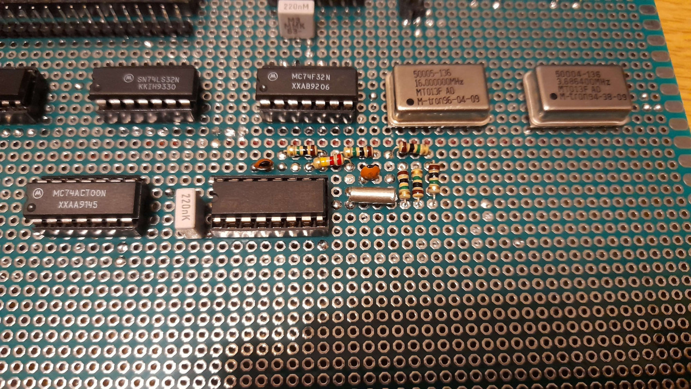
Hacked in 2048 Hz clock source
Around this time, I switched from assembly to C but I had some trouble getting it to work (I didn't fully understand how the C language worked under the hood). After experimenting with various GitHub projects, I found the m68k_bare_metal project which finally helped me succeed. This repository is well documented and includes libmetal, which provides basic C libraries - great! Shout-out to tomstorey for creating this! As for the toolchain, I used gcc-m68k-linux-gnu from my package manager (I use Debian Linux on my desktop). I had everything I needed to work in C.
My custom DOS-like OS
This computer is a custom design, so of course there won't be any existing software for it. To make it easier to work on the computer, I decided to write my own DOS-like operating system. My goal was to create a simple console file browser accessible via UART that could launch some kind of executables. As you might expect, I managed to do it. The OS consists of one large main source file in which I packed everything, from the FAT16 driver (which I had to rewrite so that it could work in a C environment and browse folders) to the command line. For the executable format, I used plain compiled binaries that were expected to load at a specific address. There is no memory management (the Motorola 68000 doesn't have memory protection capabilities anyway), so it works like x86 real mode DOS. I also created an API to call functions from the OS. I came up with the idea that the OS would fill a special table at a fixed memory address with pointers to the functions. Programs need to include the api.c file, which contains the function definitions and pointer initialization code. In the end, this system worked pretty well. Below showcase of this OS + again got the AY-3-8910 synth chip to work.
Some of these sources can be found in the GitHub repository for this project.
Going further - graphics card (TTL one!)
Having only terminal and synthesized sound was a bit boring for me. The idea to make my own graphics card struck me at this moment. While working on the 6502 homebrew project, I cheated and used a Raspberry Pi Pico. I think it was the right decision, as I was a beginner back then and did not even have the required parts to make it. As you can see above, I had hundreds of 74 logic ICs, including basic gates, counters and flip-flops. So that wasn't a problem. I also had to decide whether to make a composite or VGA video card. I don't remember exactly why, but I chose the VGA card. Maybe because it was easier? I don't remember. I started researching the most basic 640x480 VGA mode. As I researched, I mainly looked at timing diagrams because I don't like following tutorials - I prefer to build things my way!
After digging into it, I realized that VGA is actually not that difficult. It really comes down to two position counters, both clocked by the pixel clock. One clock cycle equals one pixel. These counters keep track of the horizontal and vertical position of the current pixel being drawn. At specific positions, the hardware also needs to generate HSYNC and VSYNC pulses, which happen just before the counters roll over to their maximum values. Actually, for a 640x480 resolution, the counters don’t stop at 640 and 480 - instead, they count 800 pixels horizontally and 525 lines vertically. The extra pixels are off-screen and are used for blanking and sync timing. On top of that, the graphics hardware must generate three analog signals: red, green and blue. Each one ranges from 0 to 0.7 V, representing zero to full intensity for that color. By setting these signal levels based on the current horizontal and vertical counter values, we can produce the visible image and all the colors on the screen.
To count up to 800 and 525, I needed at least 10-bit counters. From the scrap I had 74161 and 74163 4-bit binary counters. These two are almost the same - the main difference is that one has an asynchronous reset and the other has a synchronous reset. I ended up using the 74163, which has an asynchronous reset. By chaining three of them together, I got a 12-bit counter, which is more than enough for both the horizontal and vertical counters. The 640x480 VGA pixel clock is 25.175 MHz. From the same scrap I had a single 25 MHz crystal oscillator, which was good enough for this purpose since the difference is small. So the first part of the circuit consisted of two 12-bit counters, one for horizontal and one for vertical timing. The second part of the circuit was the logic needed to limit the counters and generate the sync pulses. To limit the count, I simply used a bunch of AND gates to detect when the binary counter reached a specific value and then pulse the reset. For generating the sync pulses, I used a 7474 flip-flop IC (a dual D / RS flip-flop). I used it in RS mode: when the counter reached the value where the sync pulse should start, I set the flip-flop and when it reached the value where the pulse should end, I reset it. The start and end points were again detected using AND gates. To test the design, I connected the red and green color signals to individual bits of the horizontal and vertical counters. That produced the checkerboard pattern shown below, which confirmed that everything was working.
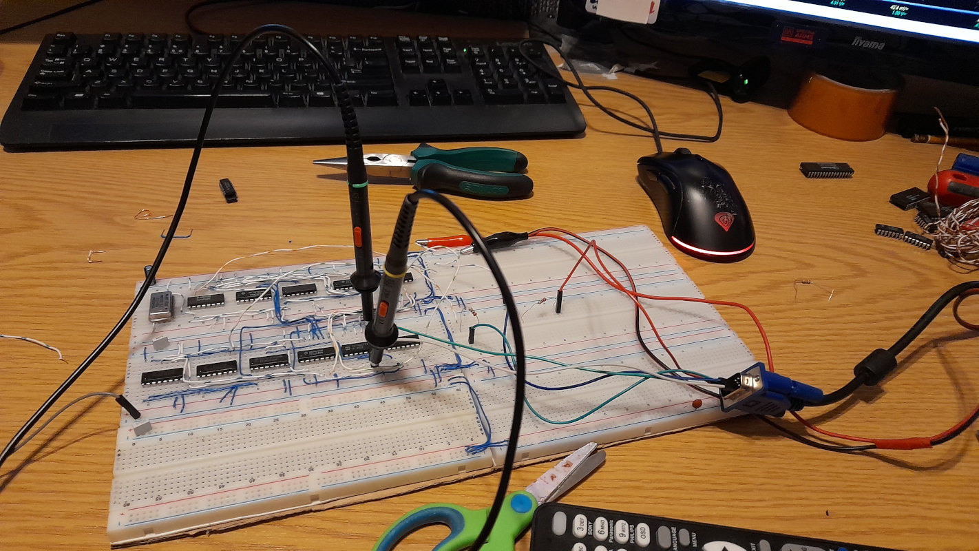
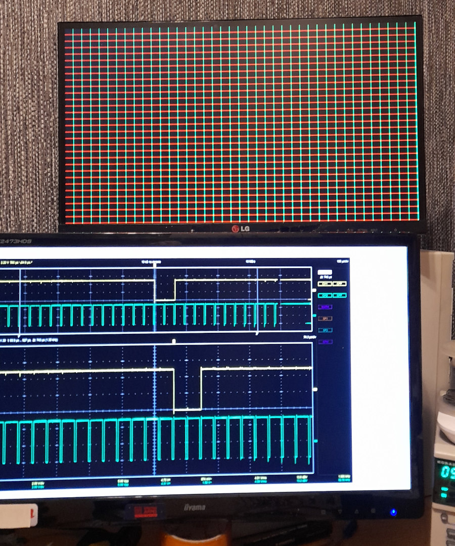
At this point in the development, I decided what this graphics card was actually going to be. I went with a single color, text only graphics card. In 640x480 resolution, using an 8x8 font, you can fit 80x60 characters. To simplify the design, I decided to go with 64x60 characters instead with the text centered on the screen. This made the third part of the circuit responsible for generating pixel data. In my scrap box I found a 4 KB SRAM chip (6264), which was enough to store data for 64x60 characters. Since each character is represented by a single byte, that part was straightforward. The next question was how to store the pixel data for each character. I still had several 2 KB 2816 EEPROMs left in the scrap and they turned out to be perfect for this job. One EEPROM can store 256 single-color 8x8 characters. Each character takes 8 bytes, because one byte stores an entire horizontal line of the character. 8*256 characters gives exactly 2048 bytes. This setup also allowed me to reduce the amount of logic needed.
I connected the first three bits of the vertical counter to the first three address lines of the EEPROM, which selects the correct line of the character during drawing. The remaining EEPROM address lines are driven by the output data of the SRAM chip (to select the character). The SRAM address is controlled by a special X position character counter (so we can center the text) and the higher bits of a vertical counter. There was one more problem to solve in the pixel data generator. The EEPROM outputs 8 bits at once - an entire line of the character - but I needed to output these bits serially, one pixel at a time. I found a solution using a 74153 IC. This chip contains two 4-input multiplexers that share the same select lines. With two additional logic gates (an OR and a NOT), I turned it into an 8-input multiplexer. The eight EEPROM outputs were connected to the multiplexer inputs and the select lines were driven by the first three bits of the horizontal counter. This way, the multiplexer selected the correct pixel from the character line as the scan progressed.
The last major piece I needed to implement was the CPU interface. I spent some time thinking about how to handle this. Dual-port RAM would have been nice, but in the end I took inspiration from early PC CGA graphics cards - CPU access would completely steal RAM access. This means that during a CPU write, the video logic loses access to the RAM, resulting in visible "snow" on the screen (I actually liked this behavior, as it felt very period correct). To multiplex the address lines between the CPU and the video logic, I used three 74157 multiplexers. Each 74157 contains four 2-input multiplexers with shared select lines (similar in concept to the 74153). For sharing the data lines, I added a 74244 8-bit buffer. Its input is connected to the lower 8 bits of the 16-bit CPU bus (addresses have to be multiplied by two) and its output goes directly to the data lines between the SRAM and the character EEPROM. The 74244 is tri-state and its outputs are enabled only during a write operation. As a result, reading from video memory is impossible because the buffer is one-way. Yes, that means I ended up making Write-Only Memory (WOM). It’s a bit of a shame, but honestly, who cares - it works.
To create the character set for the EEPROM, I wrote a small Python utility that took the IBM PC 8x8 font and converted it into the correct format, taking into account how the address lines are connected to the video RAM and the counters.
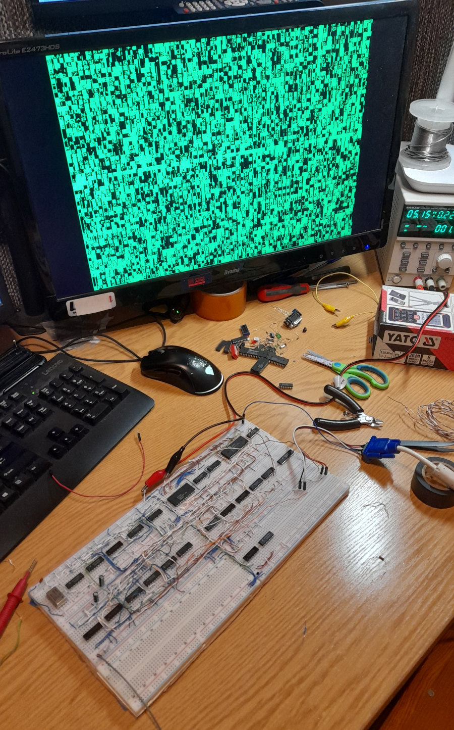
I didn't consider the timing of the parts and because of the slow logic, I ended up with vertical lines between the characters. But I didn't care! The text was readable and it's perfect for my first homebrew graphics card! I connected that breadboard graphics card to the computer with jumper wires and it confirmed that my design worked fine!
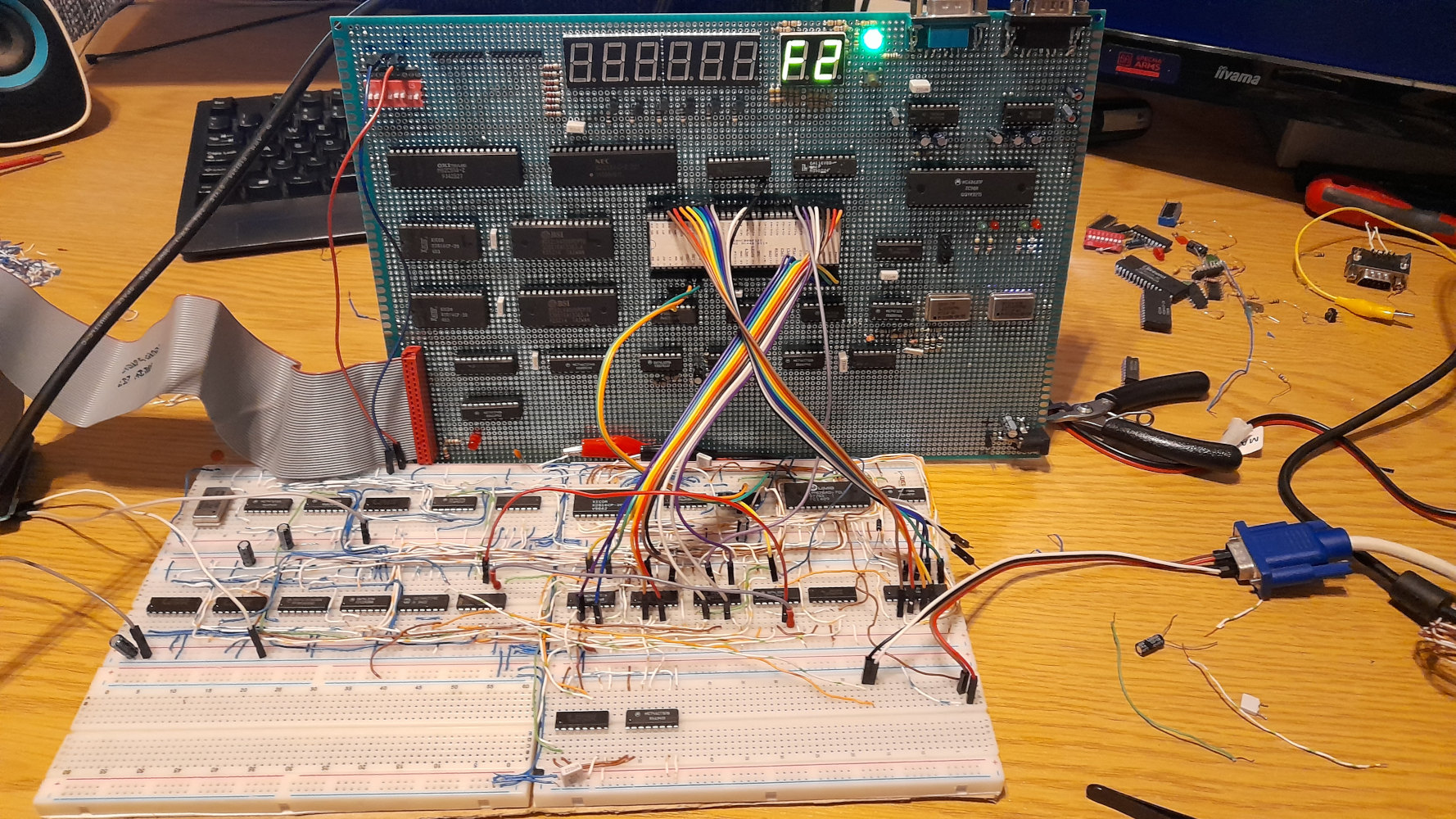
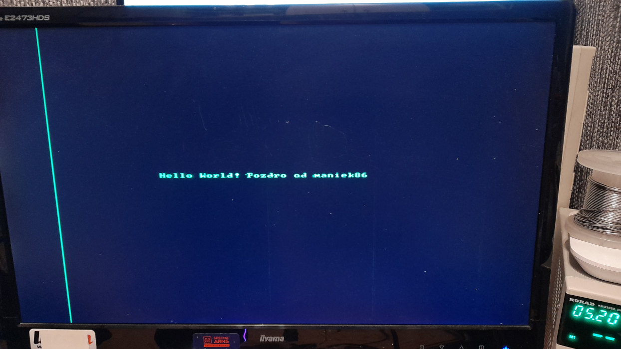
That was a short explanation of how this graphics card works. The full schematic of this graphics card is available here.
In the end, I also moved this graphics card to a prototype board. To connect it to the computer, I extracted 64-pin DIN 41612 connectors from the same scrap. With 64 pins, I could expose the entire Motorola 68000 data/address bus, so I did. I also added a few control signals and the unused outputs of the onboard 74138 address decoder.
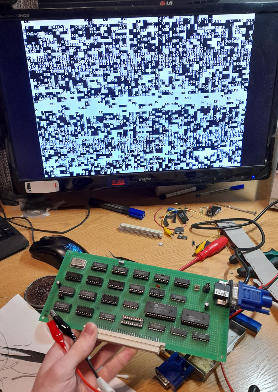
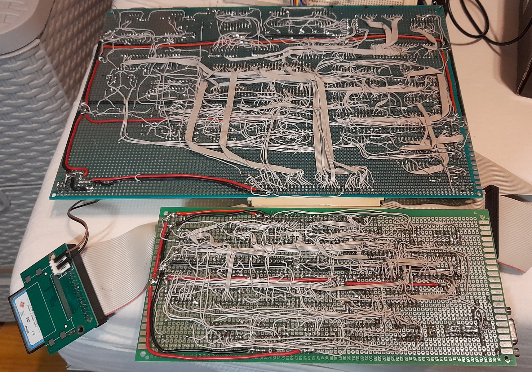
By the way, I used wire from old 80-pin IDE ribbon cables this time.
Bad Apple!!
As the heading says, I've managed to get Bad Apple running on this computer! It has sound and video, after all. It's the most impressive demo I've run on this computer, so I'm writing about it here.
Mods to the graphics card
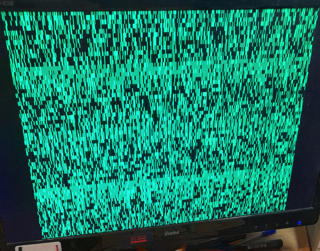
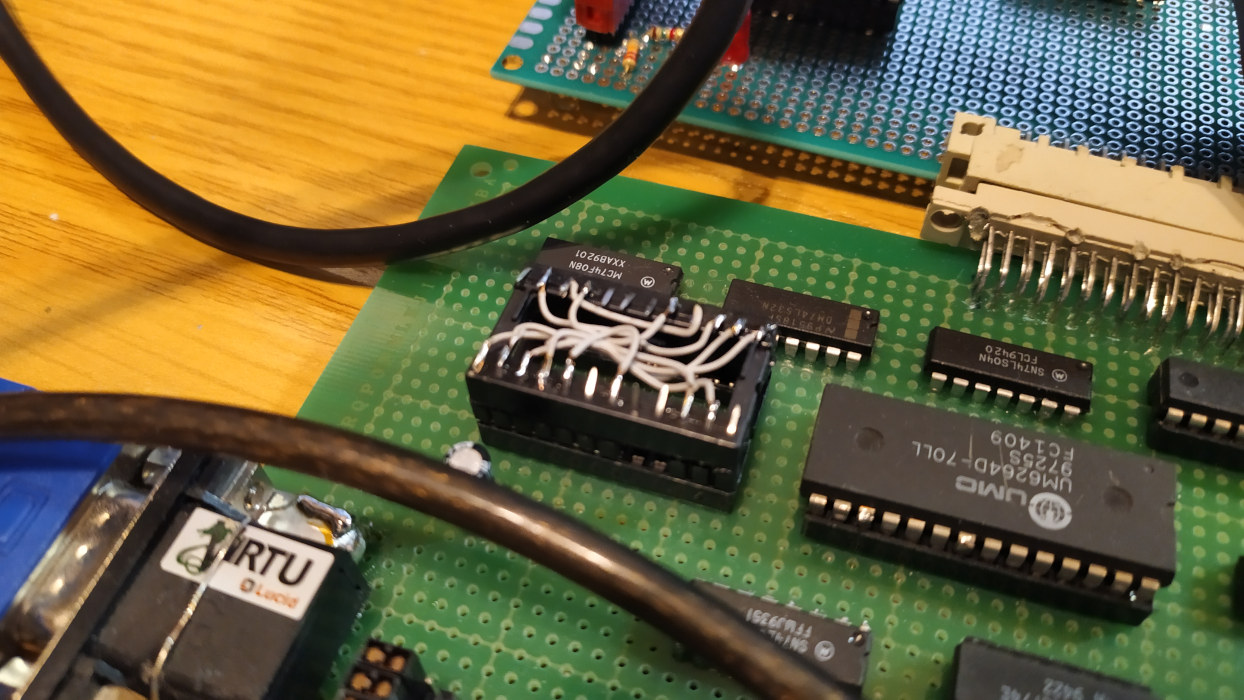
I don't think text mode is the best for video playback. As you might recall, the character generator works by connecting the video RAM output to the character ROM. The 8-bit output value indicates the current character. But what if we bypassed the character ROM? Instead of a character, we could get eight pixels. Due to the design of this graphics card, the pixels will be odd sizes: a single pixel will actually be 1x8 pixels. You will actually see that it won't look bad for that animation! So, to accomplish this, I had to essentially remove the character EEPROM and bridge the data lines from the RAM to the old EEPROM outputs. The result is shown below.
Code
The result resolution is 512 by 60 pixels. As I said, it's an odd resolution but it's not bad. A single frame at that resoltuion takes 3840 bytes (64x60). My target was 30 FPS, which means 115200 bytes per second. That's a lot! To combat this, I decided to create a simple video compression algorithm. The video data only contained information about changes (like modern video codecs do). This reduced the required data significantly! To convert the Bad Apple video into suitable data, I wrote a Python script with the help of the OpenCV library. The resulting video file was almost 3 MB. That's more than the amount of RAM we have! Plus, we need to add music later on, which weighs another 300 KB. Therefore, I decided to stream the video data off the drive. I reserved the RAM for the music. The main program has a data buffer. When the buffer is half empty, the code sends an IDE read request to the hard drive (compact flash in this case). The program doesn't wait for the hard drive to complete the read; it continues until the buffer runs out. Then, it checks the status of the drive. If it's ready, it reads the required data that got requested moments ago. This is done to reduce delays caused by the hard drive.
As for the music, the implementation was simple since I already had an AY-3-8910 player ready. I found a version of "Bad Apple" made for this chip on zxart.ee by the musician Alex Molodcov (thanks!). I slowed it down a bit to match the speed of the Bad Apple video, but in the end, it's perfect. To get the video and music perfectly synchronized, I manually adjusted the delay values in the code. After some trial and error, I succeeded! I was very thrilled to see Bad Apple running on the hardware, software and graphics card that I built from scratch. Video below!
Other upgrades
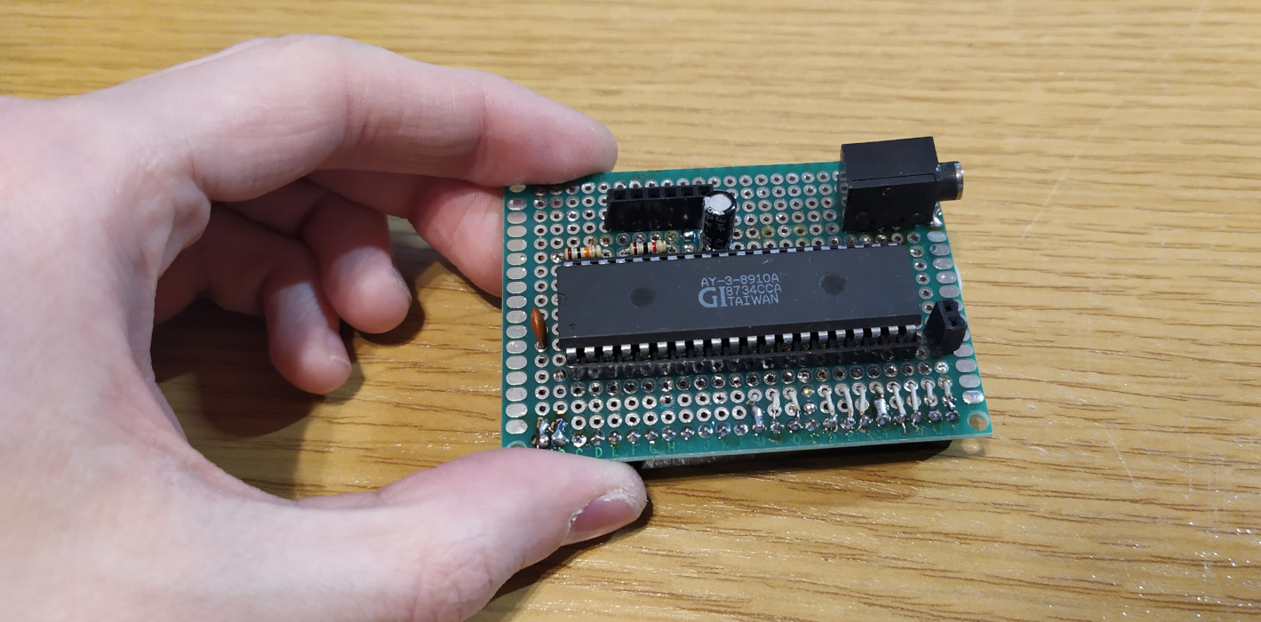
As an aside, I also wired up a dedicated PCB for the AY-3-8910 IC that plugs directly into the I/O port. The only thing that needs to be connected via a jumper wire is the clock source. It must be connected to the output of the frequency divider on the board (1 or 2 MHz output). It works nice.
Emulator
In early 2025, I decided to have some fun and write an emulator for my system. It's written in C++. It hasn't been shared with the world yet, but it's based on: SFML 2.5, sfml-widgets, Musashi Motorola 680x0 Emulator and AY-3-8910 Emulator by Andre Weissflog. It emulates the system pretty accurately, including the I/O (7-segment displays, DIP, AY chip). It can run all programs written for my SBC. I may release it in the future.


![Validate my RSS feed [Valid RSS]](http://maniek86.xyz/cmsesus/uploads/image/valid-rss-rogers.png)
