


")
![[Valid RSS]](http://maniek86.xyz/cmsesus/uploads/image/valid-rss-rogers.png "Validate my RSS feed")

M8SBC-486: Initial hardware and chipset
[Go back to the main page of this project] [Previous part]

This content may be updated as the chipset is still in development. Last updated: 06/03/2026
Chipset
The production and delivery of the PCBs took about a week. While I was waiting, I decided to start designing the chipset. Since I've worked with VHDL before, I decided to use that language.
It's worth mentioning that I had the Intel 486 datasheet (Oct.92 version) open throughout the development of this computer. In that datasheet, there is documentation and timing diagrams for all the types of bus transfer that the 486 can do. This is great, as almost no x86 chips today have documentation like this available. For simplicity, I decided to work only on the basic transfer cycles. I might take a moment to explain how 486 basic bus cycles work.

The 486 initiates a bus cycle by asserting the ADS pin (Address Data Strobe, active LOW). By doing so, the CPU also indicates that the address and control signals are valid. The actual read/write then occurs on the second clock cycle.
In our design, where there are slower devices, we would want the CPU to wait, as a read/write in the second cycle might be too fast if we operate the CPU at higher frequencies. The solution is to use waitstates. So, to add to what I was saying before, the read/write only happens when the RDY (Data Ready, active LOW) is asserted. Therefore, holding RDY inactive extends the cycle. This can be seen in the above image. It is also worth mentioning that the 486 has BRDY (Burst Data Ready, active LOW), which is used for burst transfers. In short, burst transfers enable data to be read every clock cycle. As I don't use it, I tied it to VCC to keep it inactive. The FPGA's task is basically to interpret this and translate it into control signals for other onboard devices (SRAM, 8254, 8259, ISA, etc.).
The VHDL source is therefore divided into:
- Address decoder
- BE0-3 decoder to A0/A1
- Clock dividers for the CPU, ISA and PIT
- Simple CMOS RTC implementation & NVRAM
- ISA driver
- RAM driver
- Transceiver driver
- WR/RD generator for onboard devices
- And a main file connecting all of these
VHDL source
Address decoder
Its main purpose is to decode address lines into the correct CS (chip select) signal. Its code contains CS lines for: RAM, ROM, PIC, PIT, keyboard controller, port 0x61, ISA and CMOS. It also handles the assertion of the KEN (cache enable) and BS8/BS16 (8- or 16-bit device indication) signals.
Current address map:
For the memory:
- 0x00000000 - 0x0009FFFF: RAM (first 640 KB), cacheable, 32-bit
- 0x000A0000 - 0x000C7FFF: ISA, 8/16-bit, BS8 is generated but it's later ignored
- 0x000C8000 - 0x000FFFFF: ROM (224 KB accessible out of 256 KB), cacheable, 8-bit
- 0x00100000 - 0x003FFFFF: RAM (3MB: 1MB - 4MB range), cacheable, 32-bit
- 0x00400000 - 0x0049FFFF: Empty
- 0x004A0000 - 0x004FFFFF : RAM (repeated, allows access to the 384 KB of RAM omitted by the ISA and ROM hole at 0x0000A0000 to 0x000FFFFF), cacheable, 32-bit
- 0x00500000 - 0x7FFFFFFF: Empty
- 0x80000000 - 0xFFFFFFFF: ROM (repeated, 486 execution starts at 0xFFFFFFF0), cacheable, 8-bit
I also decided to add two jumpers to the board to enable or disable the cache. One is for the RAM and the other is for the ROM. There are also two inputs to the address decoder indicating the status of these.
For the IO:
- 0x20 - 0x21: PIC (Programmable Interrupt Controller)
- 0x40 - 0x43: PIT (Programmable interval Timer)
- 0x60 and 0x64: Keyboard controller
- 0x61: 0x61 IO port
- 0x70 - 0x71: CMOS
- And all else is mapped to the ISA
BE0-3 decoder to A0/A1 (be_decoder.vhd)
Since the 486 is a 32-bit processor, it does not include A0 and A1, which are used for 8/16-bit devices. We can generate these address lines based on the four Byte Enable (BE0-3) pins. During a normal 32-bit transaction, they indicate which bytes of the 32-bit data bus the data is present on/accessed. They are also used for 8/16-bit transfers to indicate what is being transferred in split transactions.
The 486 datasheet provides an example of how to implement this, so it only took a few moments to implement it.

Clock dividers for the CPU, ISA and PIT (clock_section.vhd, clock_section_pit.vhd)
There are two files for each device that needs to be clocked: The CPU and the PIT (ISA is clocked by isa_driver.vhd). There are two crystal oscillators on the board: One is 48 MHz and the other is 14.138 MHz. Both clocks go into the FPGA. The 14.318 MHz clock also goes to the ISA OSC pin. The 48 MHz clock is used to generate the CPU clock. By dividing it by 4.0, I get 12 MHz, which I have decided will be the CPU frequency for the initial tests. The second clock is divided by 12 for the Programmable Interval Timer (PIT). Later I experimented with increasing the CPU clock and achieved good stability at 24 MHz (DX2 CPUs run at 48 MHz then!). It's difficult to go any further because the FPGA software indicates that the worst delays are about 25 ns, while the period time at 33 MHz is ~30.3 ns.
Simple CMOS RTC implementation & NVRAM (CMOS.vhd)
I decided to implement a minimal RTC for various existing software. It's nothing special - it acts similarly to the classic CMOS from the x86. The CMOS contains two registers: data and address ports. This implementation simulates that functionality. There are time and date counters in the file. It's clocked by a PIT frequency that is divided to give an exact 1 Hz. Later on, I also added to this file the implementation of 32-byte CMOS nonvolatile RAM, which holds the BIOS configuration. I realized that two of the five configuration lines that the ATmega128 uses to load a bitstream into the FPGA could be repurposed as general I/O later on. I used these two lines to transfer data between the FPGA and AVR, which allowed me to store the FPGA CMOS memory in the AVR EEPROM. Upon powering on, the ATmega128 restores the configuration. This was accomplished by creating a custom two wire protocol with clock and data lines to transfer data serially.
I think it's a pretty interesting idea to store CMOS settings with an ATMega128 microcontroller. Below is an explanation of how it works.
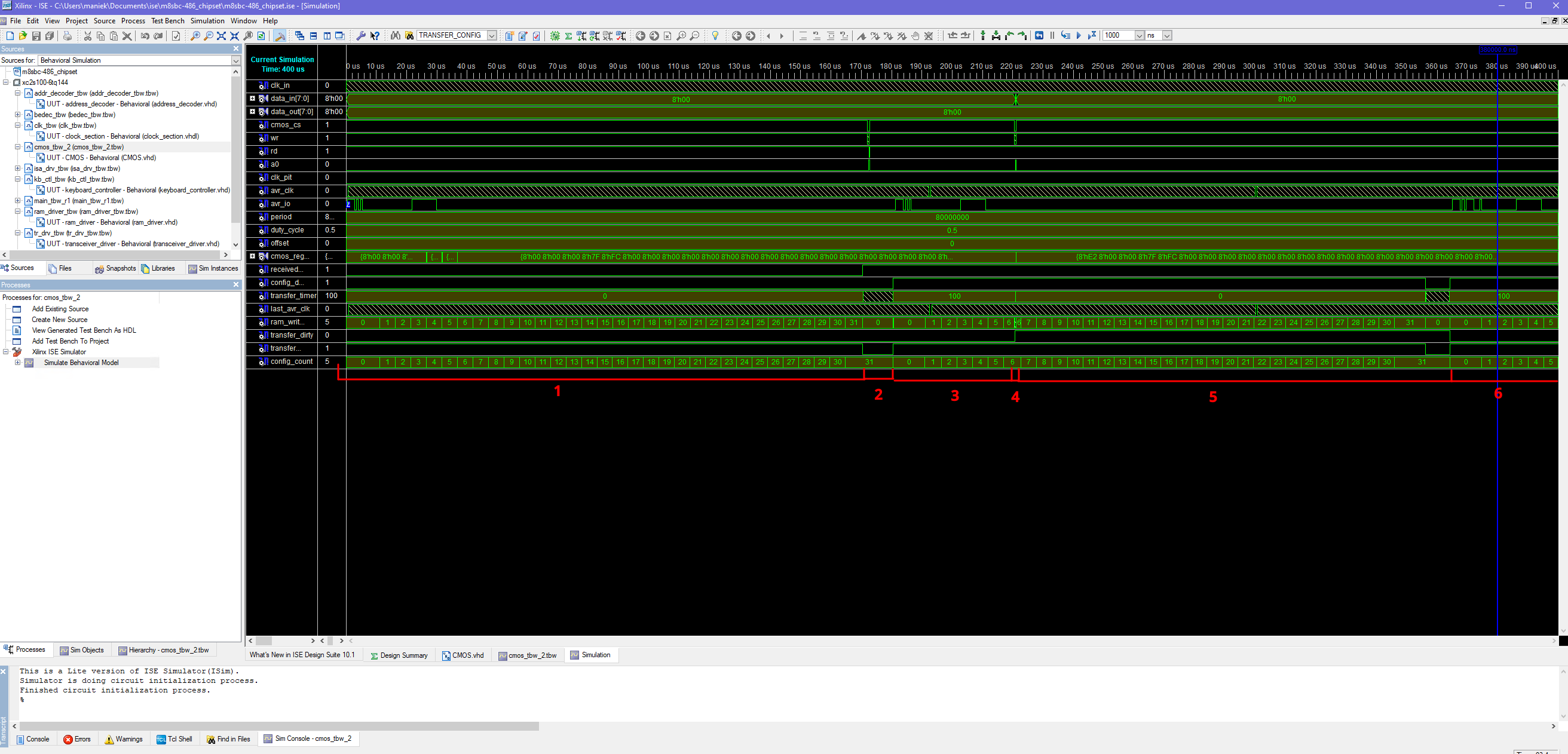
In the M8SBC-486 project, the ATMega128 mainly stores the FPGA's bitstream. Upon powering on, it sends the bitstream to the FPGA via a few configuration lines. However, two of these lines can be used as input/output (I/O) pins after configuration. I decided to try using them for communication between the FPGA and the ATMega. Why? The ATMega has an EEPROM that we can use to store "CMOS" settings. Since the FPGA is not a microcontroller, implementing standard communication is more difficult. Therefore, I created this simple protocol to keep the VHDL code "simple" and free of dependencies. The screenshot above shows:
- This is the moment after the bitstream loads. The FPGA CMOS section waits for the ATMega to send the stored CMOS configuration via these two lines. The ATMega generates the clock, allowing both devices to sync. One line is the clock, and the second line is the data. It waits for the "F5" byte on that two-wire bus. After receiving that byte, it expects 32 bytes of CMOS data (CMOS can currently store 32 bytes). After receiving all the bytes, the ATMega continues clocking, but turns into a listener because the FPGA will send data later.
- This is the idle state. The FPGA stores the CMOS and the CPU can easily read it from the internal RAM. If a write occurs to the CMOS data, it is marked as "dirty". When the CMOS is "dirty", a count begins. If the counter reaches the preset value, it goes to step 3. However, if other writes occur, the counter resets (in case the CPU updates multiple CMOS bytes at once). In the test bench, the value was set very low, but on the board, it's set to like 100000 clock cycles.
- The count reaches the preset value. The FPGA begins shifting the CMOS data out to the AVR, which stores it in its EEPROM. First, it sends the "F5" byte to the AVR. Then, it sends 32 bytes of CMOS data, followed by the confirmation byte "AA." If the ATMega sees the "AA" byte as the 34th byte, it writes the buffered CMOS data into its EEPROM.
- But what if the CPU writes data during the transfer? Or in general, if it tries to access the CMOS RAM? We can't have two devices access one RAM simultaneously (I configured the CMOS to use a single-port RAM in the FPGA). Let's just steal the access from the configuration writer!
- In that case, the rest of the bits sent to the AVR will be 0 because the writer can't read the FPGA's CMOS RAM since it's occupied. This means the confirmation byte won't be "AA", causing the AVR to discard the data.
- Since the previous transfer was unsuccessful, we wait for the counter to finish (it was reset after the previous transfer) and try again.
ISA driver (isa_driver.vhd)
This one was more difficult to implement. The 8-bit ISA is easy to implement; however, this time, I also decided to implement the 16-bit ISA. The 16-bit ISA requires kind of a "handshake" for 16-bit transfers, as well as a more complicated state machine that checks for that capability before the transfer begins. Additionally, the ISA is a slow bus, so many wait states were required to make it work properly. Because of the dynamic bus sizing, this driver generates BS8 and BS16 on its own.
Later note: The initial driver was asynchronous to the ISA clock. This was fine for the initial tests I ran with my Trident TVGA8900C graphics card, which seems to be pretty resistant to uneven ISA implementations. However, issues occurred when I started testing other graphics cards. Writes and reads were broken resulting in cards that either did not work or initialized only in 8-bit mode, which greatly reduced performance. In late February 2026, I rewrote the ISA driver based on the book titled "EISA System Architecture Second Edition by MINDSHARE, INC. TOM SHANLEY DON ANDERSON" (1995). Although it is a book about EISA, it also explained basic ISA transfers with a timing diagram which allowed me to properly implement the machine state for ISA. The new ISA driver uses the CPU clock to divide it into an ISA clock. This approach enables the creation of a driver without the need for "clock cross-domain synchronization".
RAM driver (ram_driver.vhd)
I decided to use SRAM because it is easy to drive. We simply input an address and optionally, data, and then read or write with a strobe signal on an OE or WE pin. The RAM driver has its own file due to the organization of the memory on the board. A 32-bit 486 CPU works best with 32-bit memories, of course. With eight 8-bit, 512 K SRAM chips, I split them into two 2 MB banks. Each byte has an OE and a WE line. In total, we have OE0-OE3 and WE0-WE3. To address the correct bank, there are two CS lines.
Transceiver driver (transceiver_driver.vhd)
As I explained in the previous part, in order to interface a 32-bit 486 with 8- or 16-bit devices, we need a way to place the 8-bit bus data on the correct bytes of the 32-bit bus. This part listens for the BS8, BS16, and BE0-BE3 signals and controls the chip enables of the four transceivers to move the data correctly. I included a reference image from the datasheet below.

WR/RD generator for onboard devices (wr_rd_generator.vhd)
Intel-style peripherals use RD/WR strobes to read or write data. To transfer data from/to the device, we simply put the correct address lines and then do a pulse on the RD or WR pin. The device will then make the data available or write it during that pulse. This part implements that functionality. Initial tests also used it for ISA (8-bit), but I moved it into a dedicated section when I needed to implement 16-bit. This part mainly generates IO reads/writes to the onboard peripherals and a MEM read signal to the ROM. The MEM write capability ultimately became unnecessary because we have the RAM and ISA drivers for memory writes.
And a main file connecting all of these (m8sbc_main.vhd)
The main file contains all the definitions of the pins, internal signals, incoming signals and outgoing signals. In that file, I also multiplex various signals because some output signals can be driven from multiple sources (one at a time, depending on the conditions) I also set the amount of wait states for the drivers here. Lastly, it's the perfect place for quick temporary fixes!
Issues
Here's a list of hardware/chipset issues that are still present or have been resolved.
Present issues:
Flaky compatibility with ISA cards & ISA BALE issue:
Some ISA cards simply don't work and I'm not entirely sure why in some cases (I haven't investigated this extensively). For some ISA cards, especially the 16-bit ones, one of the main reasons is that the BALE (Bus Address Latch Enable) pin is tied to ground. Tying it to ground makes the latch always active and passes the address because the address doesn't change during a bus transaction. However, some cards require a pulse anyway. I later read (after manufacturing) that the extra address lines of the 16-bit ISA extension are valid when this signal is high. Even now, I am still confused about the full purpose of this pin. This problem can be solved on some cards by taping the BALE pin. It is difficult to solve this issue, even by cutting traces on the PCB because there is an internal GND layer.
L1 cache is broken on ROM:
Enabling the L1 cache on the ROM results in random RAM corruption. I haven't looked into this a lot yet.
Rare crashes with some configurations:
Honestly, I sometimes don't know. These appear randomly. Might be hardware, BIOS or software related. They might be related to the hardware, BIOS or just software.
Fixed Issues:
L1 cache is broken on RAM:
When enabling the L1 cache, especially on the RAM, it either fails the initial 64 KB RAM test or corrupts the memory.
The fix: Allowing the 486 to cache the current bus cycle (the KEN signal is active during the bus transfer) enables the 486 to convert the normal bus cycle into a cache fill bus cycle. This cache fill fetches 16 bytes of data in four transfers. I found out later that the datasheet mentions that during the first cache fill transfer, BE0-BE3 should be ignored. In the initial design, the OE pins were tied to the BE pins to request only the data wanted by the CPU. Tying these to 0 (enable) during a read made the L1 work! This means that, even with a single-byte read from memory all RAM chips will be active. That doesn't really matter because the 486 ignores the data on the rest of the lines.
Broken ISA transfers:
Some cards (especially graphics cards) hate my current ISA implementation and they refuse to use 16-bit transfers, corrupt writes or corrupt reads. I highly suspect this because of my quickly done ISA driver. It's enough to get 16-bit transfers on 16-bit IDE to work, but not enough to make graphics work reliably. Some graphics cards (for example, my TVGA8900) can be forced to do 16-bit transfers after they got initialized in 8-bit mode by tweaking its registers. Currently, the ISA driver works asynchronously to ISA CLK (it just adds many waitstates for the CPU to simulate the correct WR / RD signals hold times), so the fix will require larger rewrites. It's TODO for the near future.
The fix: Rewrote the ISA driver to synchronize with the CPU clock.
Last updated: 16/05/2026