M8SBC-486: Introduction, schematic and PCB design
[Go back to the main page of this project]
Intro
During the summer of 2025, I worked a little more on my 486 homebrew computer, which was built on a prototype board. I quickly realized that the specs of that computer were not great, so I decided to create something better. I slowly started sketching something in my free time sometime in August. Some time before that, PCBWay had sponsored me for my smaller projects (ISA cards). I thought maybe I could ask them to sponsor one more, larger project. I asked, and they agreed! This gave me a lot of motivation to actually make something out of this. So, I decided to finish it.
Schematic
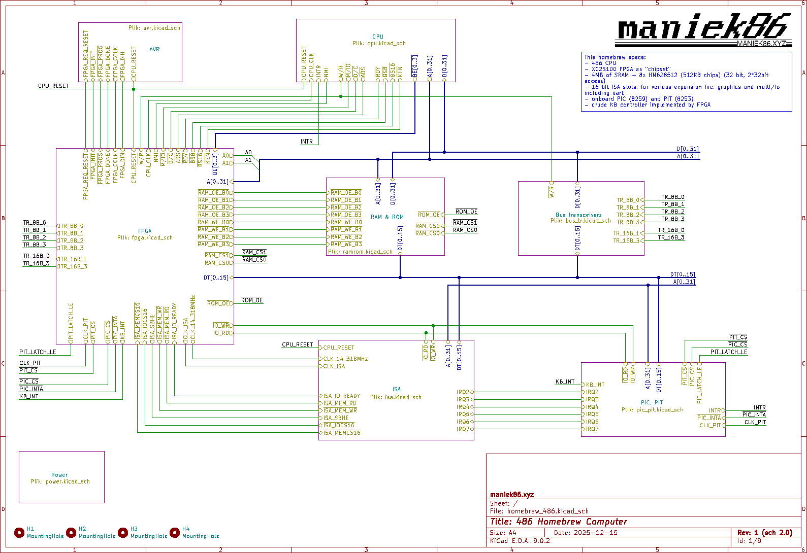
As for creating the schematic, I had experience with KiCad from a previous projects, so creating a larger schematic was not such a big deal for me. I also had experience with the 486. I broke down how I made the schematic into points that correspond to pages on the schematic. I have included images of the pages below. Full high resolution schematic in PDF is available on the GitHub.
Page 1: Main sheet & system architecture
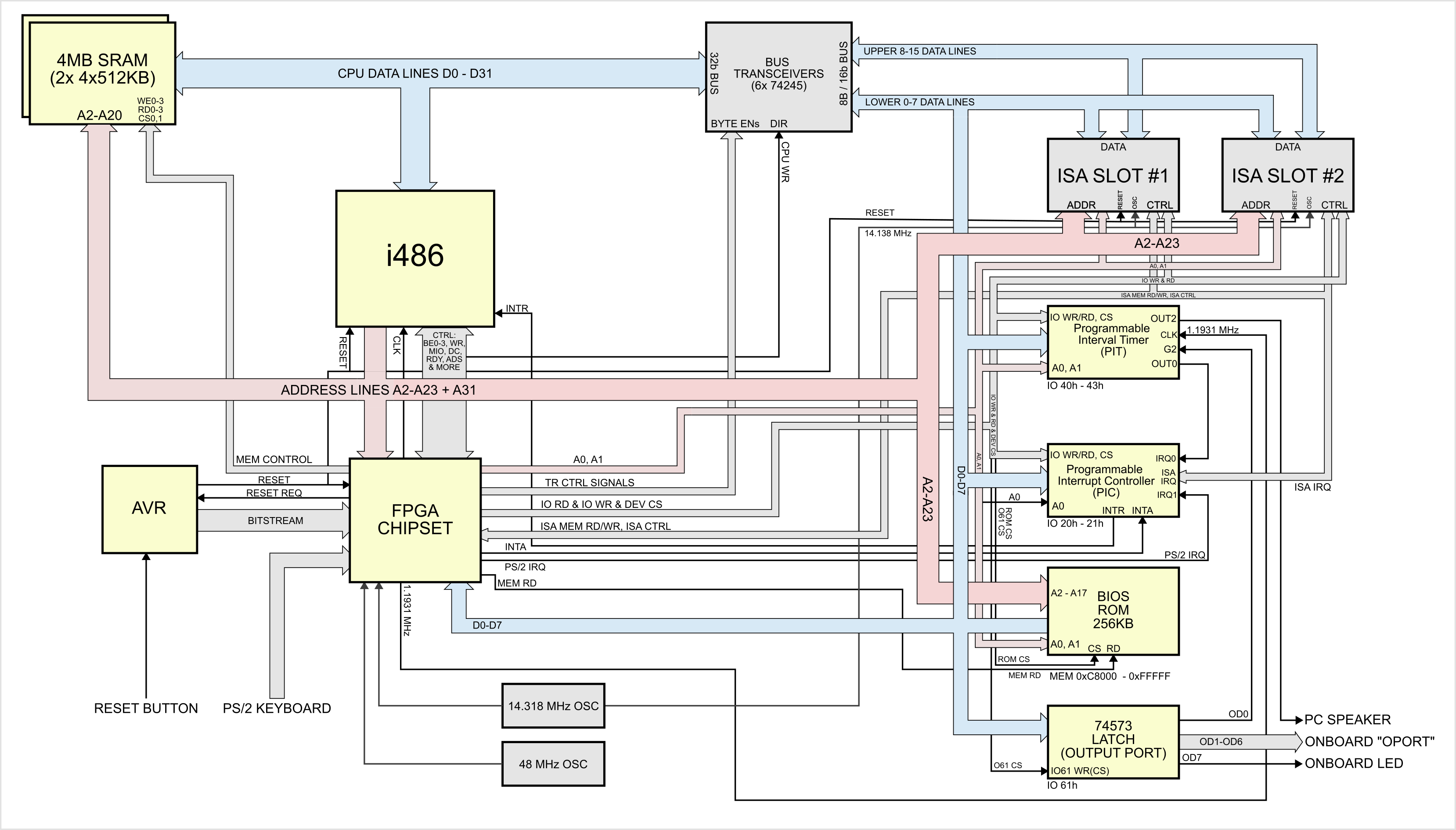
This page contains sub sheets of the rest of the schematic. It also shows nicely how components relate to each other.
Pages 2, 3 and 7: Power, CPU and bus transceivers
CPU:
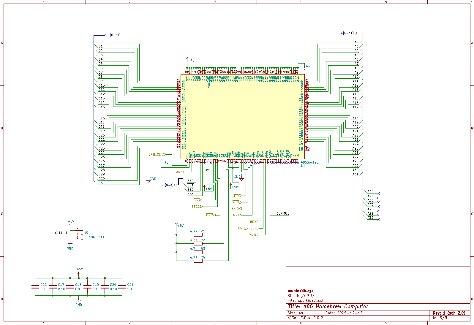
For the entire system to function, we need the main CPU - the 486. Most 486-compatible CPUs use a 17x17 pin grid array socket with 168 pins. Therefore, we need a symbol and a footprint for it. Thankfully, I found an existing project online which provided me with that. After importing it, I connected all the power signals first. For the first revision, I decided to connect the CPU power to 5V. I know that limits me from using DX4 and later CPUs, but I didn't want to complicate everything back then. Next, I connected the address and data lines to the buses that I would use later. I decided not to use all the address lines because I knew I wasn't going to use the full 4 GB addressing capability of the 486. After that, only the control lines were left. From the previous project, I knew more or less how to connect them and which ones to use. I also knew which ones to tie to power/ground and which ones to leave unconnected. Most of the connected lines went to the FPGA. You can also see that there are 4 resistors - these are for parity. The datasheet for the 486 says that these can be pulled high if parity is not being used.
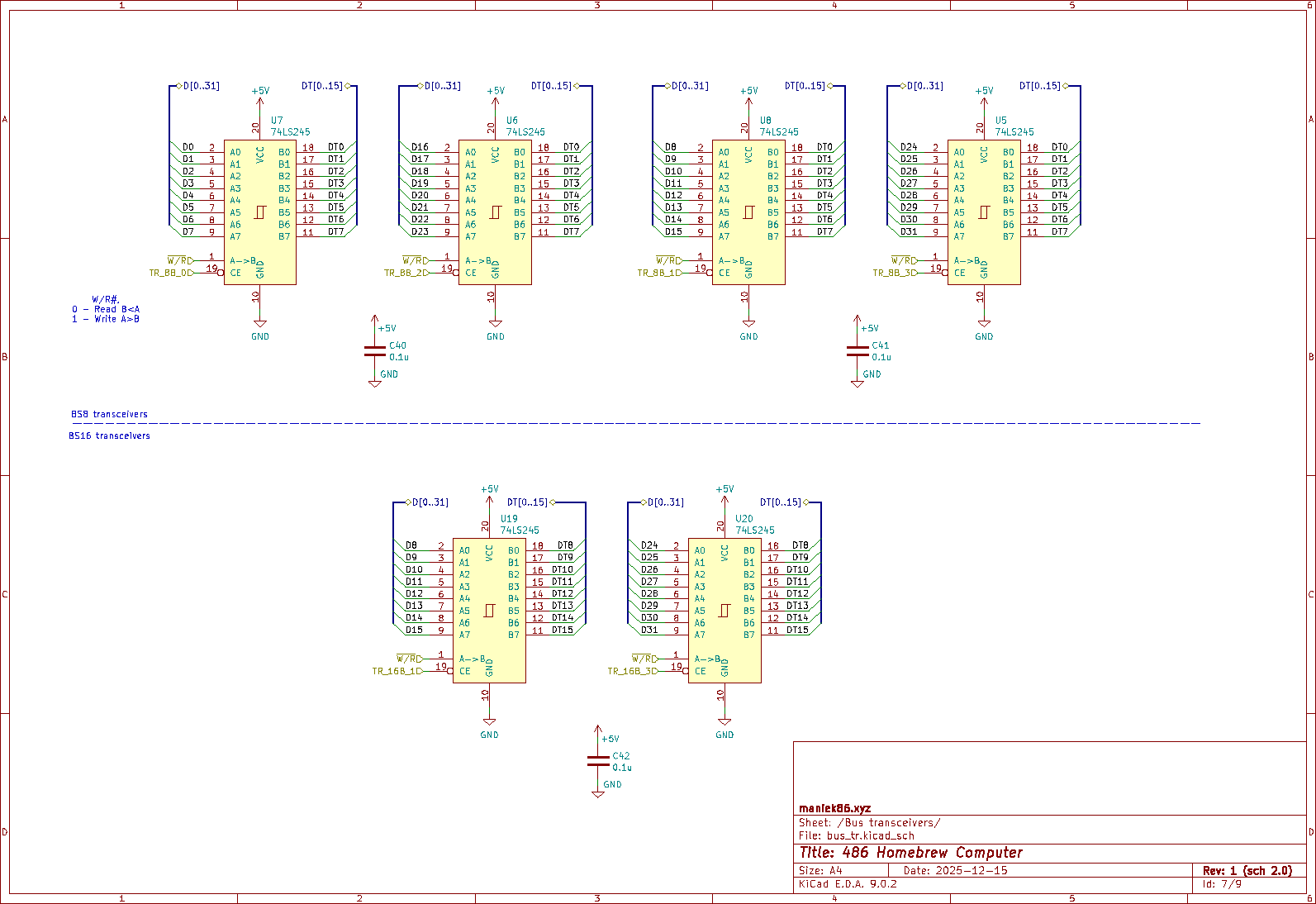
Six 74245 transceivers:
The 486 bus is 32-bit wide. Thankfully, Intel implemented something called dynamic bus sizing in the 486. This allows us to split a 32-bit transfer into four 8-bit transfers or two 16-bit transfers. During a transfer, we just have to activate the BS8 or BS16 signal. However, there's a caveat: for bus transfers that are less than 32 bits wide, we must forward the 8-bit data to the correct byte of the 32-bit data, based on A0/A1 (A0 and A1 are decoded from BE0-BE3 signals). For example, if the CPU requests a 16-bit value from an 8-bit device, we must activate BS8. The CPU then splits the transfer into two 8-bit transfers. For the first transfer, the CPU expects data on bits 0-7 of its data lines, but for the second transfer, it expects data on bits 8-15, not bits 0-7 again! These transceivers are controlled by the FPGA. I could do this directly in the FPGA, but that would require 32 + 16 pins, so using dedicated transceivers was more efficient. So, basically these put bytes from 8 or 16-bit devices correctly on the 486's 32-bit bus.
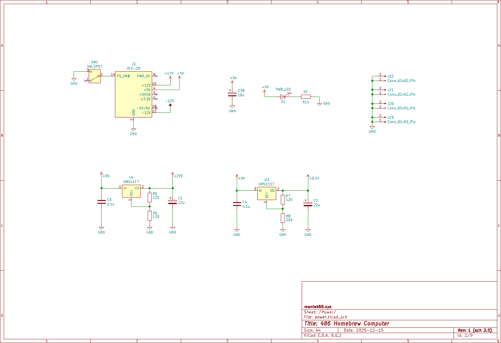
20 Pin ATX power:
ATX is pretty much today's standard in terms of computer power. I decided to use the 20-pin power connector because I had one in my spare parts bin. I could go with 24-pin, but I thought that I didn't need it - and anyway, it's not like this board is going to draw a lot of power. I used the ATX power pretty simply. I didn't use +5V SBY or PWR GOOD. To turn on the PSU, I added a two-pole switch. I also added a LED to indicate power.
Voltage regulators:
In terms of power, Xilinx Spartan II FPGA needs two voltages: one for the core and one for the I/O. The core is powered by 2.5V, and the I/O can be powered by anything from 3.3V to 1.2V as far as I remember. In my design for the I/O I need to use 3.3V. I used inexpensive LM1117 adjustable voltage regulators to generate these voltages from 5V. I could have taken the 3.3V from the ATX power, but since I wanted to do initial tests with a single voltage lab power supply, I decided to just make the 3.3V work off the regulator.
Other:
From other stuff there are:
- CLKMUL select jumper: I was not fully aware of what the CLKMUL pin does, so I decided to break it out instead of tying it to power or ground.
- Four 2-pin GND connectors: I placed them on the edges of the board later on to act as optional stands (similar to the way they are made on STM32 Nucleo boards). These can also come in handy for debugging, as they expose the GND (e.g., for a scope probe).
- A bunch of capacitors: for decoupling and better stability.
Pages 4 and 5: FPGA chipset and AVR
Xilinx Spartan II FPGA and ATMega128:
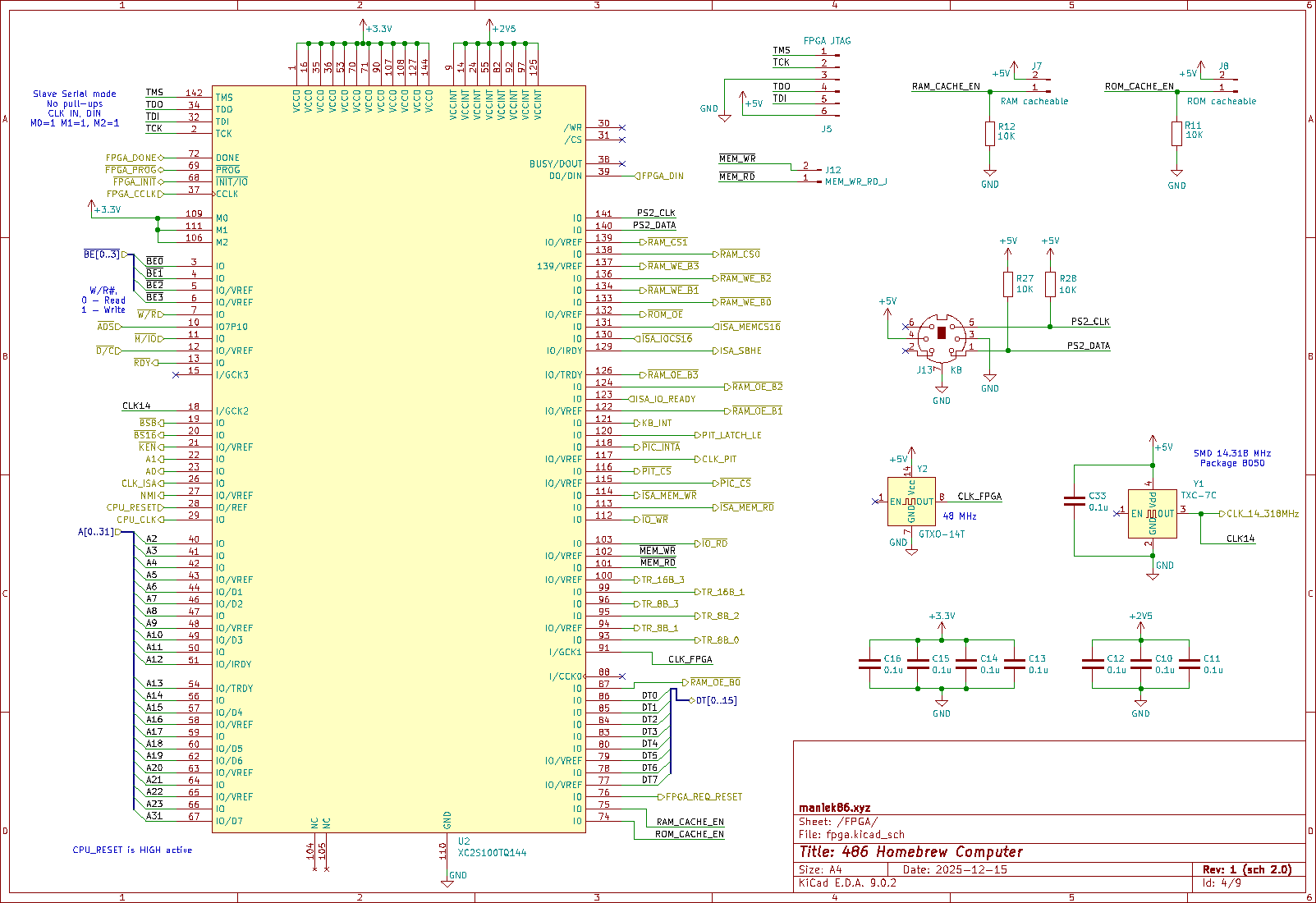
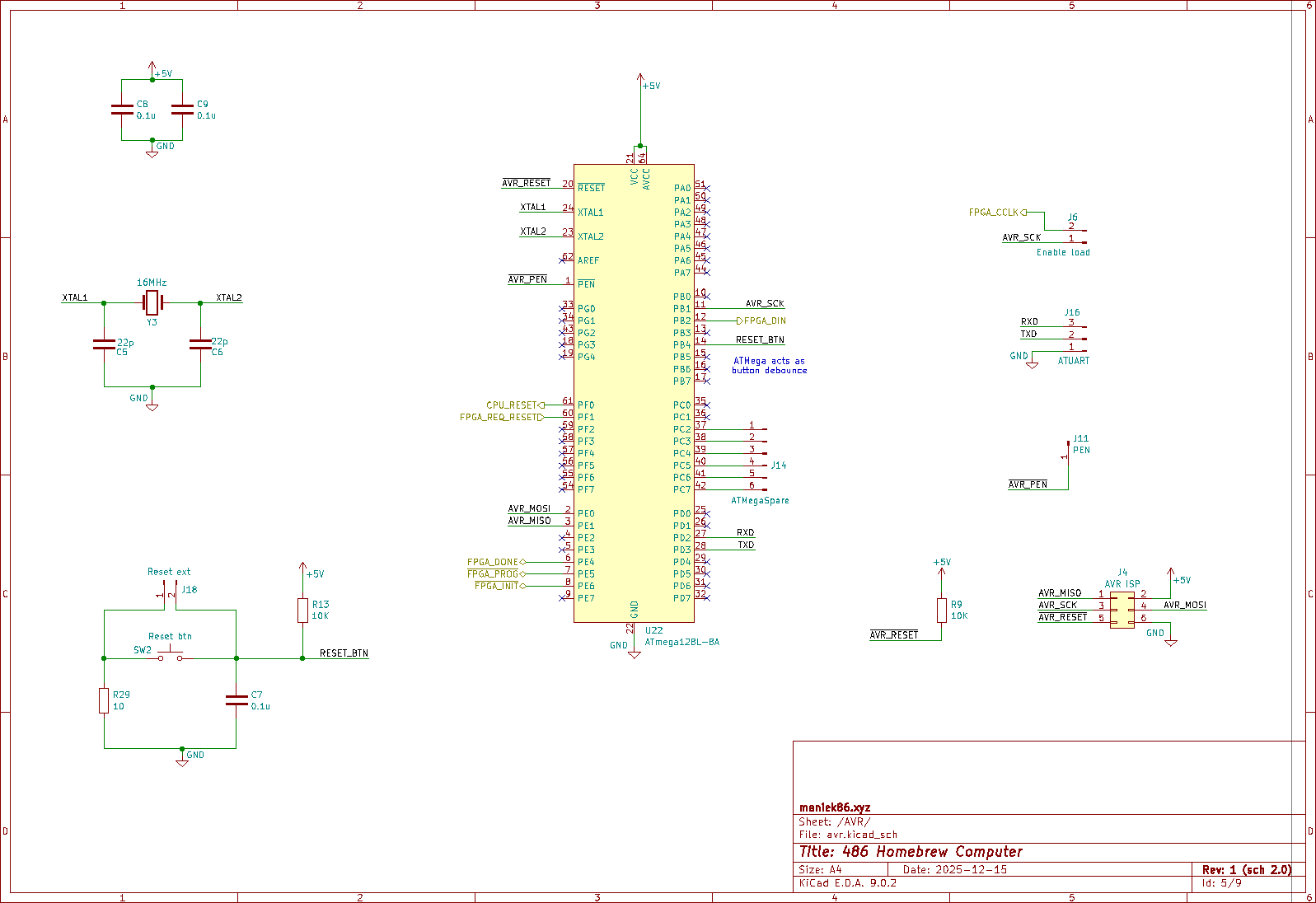
This is a crucial part of the project. XC2S100 in TQFP144 package, gathered from scrap. I used a solution similar to the one used in the prototype 486 homebrew computer, which was a programmable logic device. I previously used a XC95144XL CPLD. CPLDs have their own flash memory to store the configuration. However, FPGAs do not. They need something external to load a bitstream (configuration) into them. This can range from dedicated ROMs to microcontrollers. The XC2S100 FPGA bitstream size is 96 KB. From the same scrap where I found the FPGA, I also found an ATMega128 microcontroller. I noticed that there was no dedicated configuration ROM in that scrap. Upon further inspection, I discovered that the FPGA's configuration pins were connected to the ATMega128. Without further checking, I realized that the ATMega128 in that solution loaded the bitstream, which was clever! The ATMega128 has 128 KB of flash memory, so the 96 KB bitstream would fit without a problem. I decided to experiment with this while making the schematic and had a working prototype within a few hours. As mentioned, there are a few ways to configure the FPGA. For example, it can generate a clock signal (be the master) and read the bitstream data on a few I/O pins, or it can be clocked by something external (be the slave). I used the second option. Essentially, the ATMega sends the bitstream to the FPGA bit by bit. To speed up the entire operation, I realized that I could use hardware SPI for a very fast upload. I tweaked my experimental code to use hardware SPI, and it worked like a charm. The time it took to initialize the FPGA dropped from about a second to less than 100 milliseconds.
At that point, I also started thinking about the reset circuit and power-on reset. There was still plenty of space for code in the ATMega128, and most of its pins were unused. I decided to use it to handle the reset. In the final design, the global reset comes out of the microcontroller. In the end, I made three reset sources. The first is the power-on reset (POR). While the ATMega loads the bitstream, the reset is held active and cannot be released until the bitstream is successfully loaded. After that, the other two reset options unlock. The second is the reset button. And the third is a direct reset signal from the FPGA. I decided to route one I/O from the FPGA to the microcontroller to allow the chipset to reset the entire device when an error occurs or when the software requests it.
Lastly, as for the ATMega128, I made headers for ISP programming and UART for debugging, as well as a few unused pins.
Moving back to the FPGA, I like the Xilinx Spartan II family because its I/O pins can tolerate 5V when set to input. This means that I don't need to use many I/O level shifters and I can in most cases, connect things directly to it.
The first half of the I/O pins are directly connected to the CPU, such as the control and address signals. I also connected eight data signals coming from data width-reducing transceivers. This allowed me to implement additional functionality for the entire computer in the chipset, if needed. The second half went to other onboard devices.
In that initial design, the FPGA is responsible for the following:
- Handling, decoding 486 bus transfers
- Decoding addresses (SRAM, ROM, ISA, and onboard devices)
- Driving the SRAM
- Decoding BE0–BE3 into A0 and A1.
- Generating clock signals (dividing 48 MHz for CPU CLK and 14.138 MHz for onboard devices)
- Handling interrupt acknowledgment from the CPU
- Driving the ISA
- Driving the PS/2 keyboard (keyboard controller)
As mentioned above, I decided to implement a PS/2 keyboard controller in the FPGA. To do so, I added a connector and connected signals to the FPGA. Similar to the ATMega128, I made headers for JTAG and two configuration jumpers (caching enable). There is also a jumper to disable bitstream loading.
Pages 8 and 9: Onboard devices and ISA
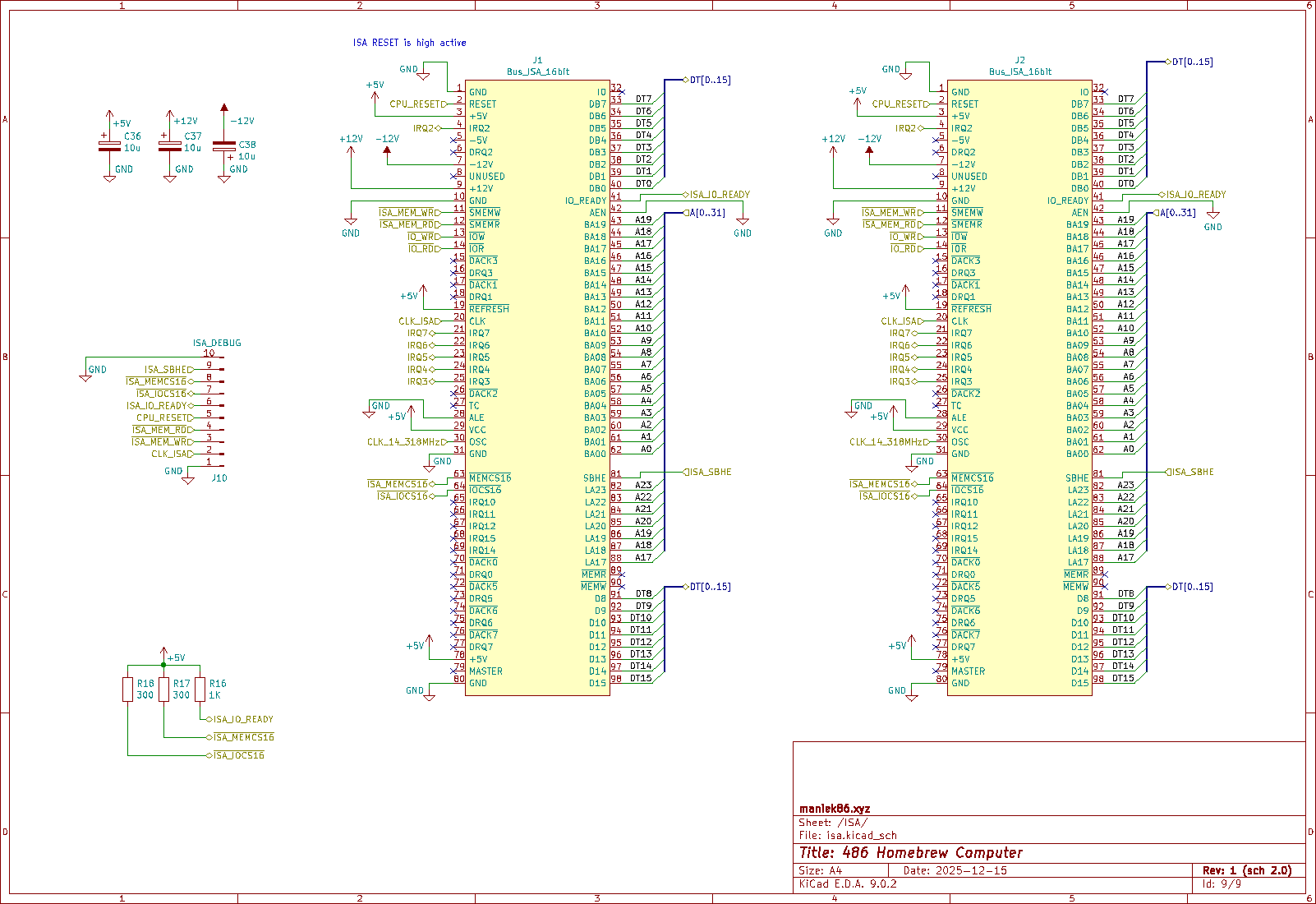
8259 Programmable Interrupt Controller (PIC):
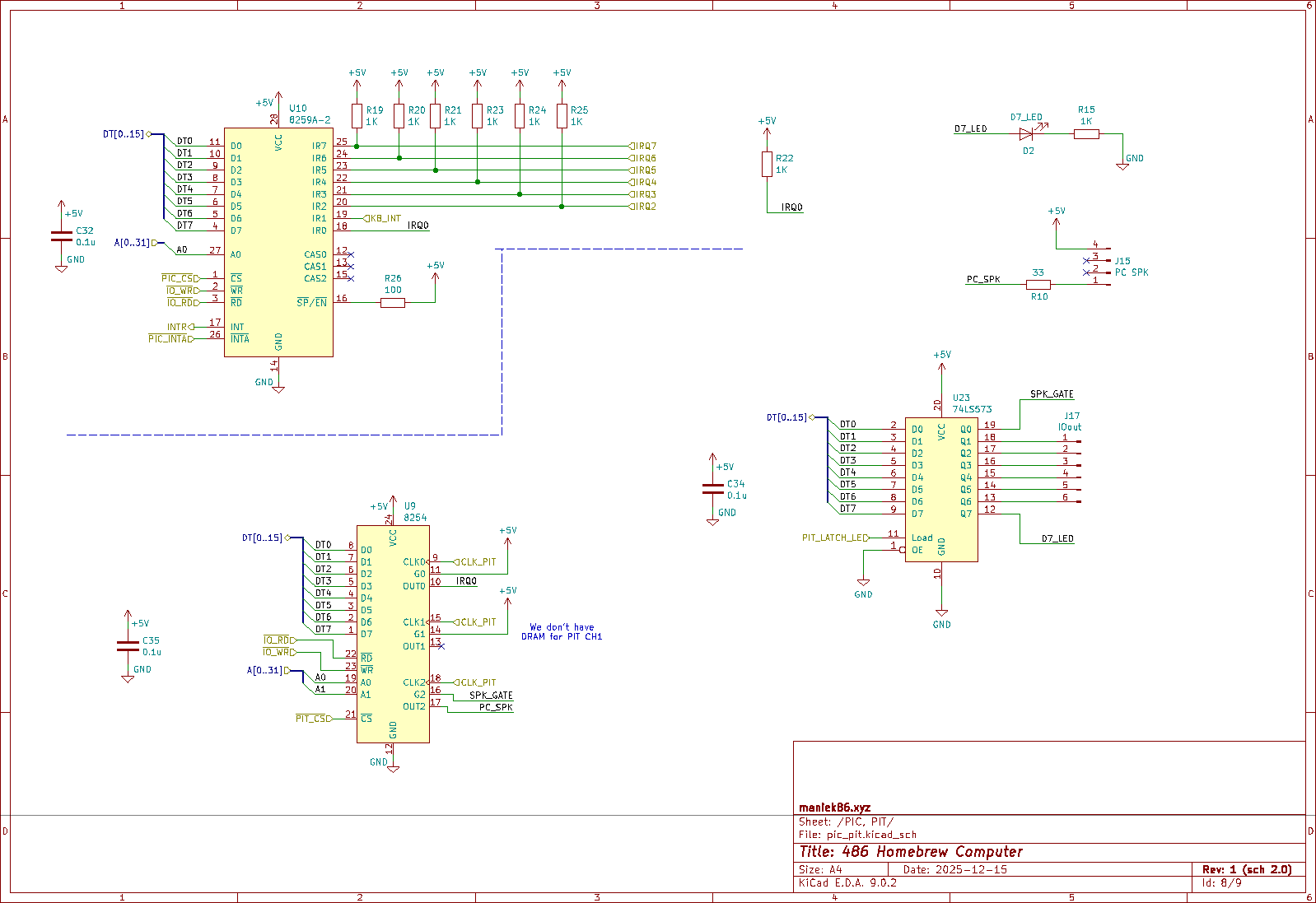
A classic x86 programmable interrupt controller. At the time of design, I didn't have much experience with hardware interrupts, especially with multiple. I had only experimented with single non-maskable interrupt (NMI) in the previous project, so I wasn't fully confident that this design was correct. I simply followed the 8259 datasheet. The FPGA generates an interrupt acknowledge signal as the 486 indicates it by making a special bus cycle.
8254 Programmable Interval Timer (PIT):
Timers are a crucial part of many systems. I had never interacted (electrically) with an x86 PIT before, but it wasn't hard to connect it properly. I decided to make it work like it does in standard PCs: I clocked it at 1.1931 MHz and connected channel 0 to IRQ 0 and channel 2 to a speaker.
74573 8-bit D-Latch:
On standard PCs we have I/O port at address 0x61, which is primarily responsible for turning the PC speaker on and off (bit 0). Since this is done by controlling the 8254 timer GATE pin, I decided to implement it using a latch. Using latch made this I/O port write-only, which might sound funny. To prevent undefined behaviour, I decided to capture the data with the FPGA during writes. In the case of a read on that port, the FPGA will respond with that data. Additionally, I added a debug LED to bit 7 of the port and exposed the remaining six bits to a special pin header.
Two 16-bit ISA slots:
Two ISA slots might be a low amount of expansion for a system where nothing is integrated onto the board. I decided to use two slots so that all elements would fit on the PCB. Two slots are also ideal for having just a graphics card and a multi-I/O controller. Since I consider this computer to be experimental, I think that is enough for now. Additionally, the ISA can be extended with risers - there is nothing specific to individual ISA slots because ISA is a bus. The ISA is also the only "device" on the board that uses a 16-bit translation feature of the transceivers section.
Other:
From other stuff there are:
- ISA debug header: Header which exposes some ISA signals. In previous projects, I only worked with 8-bit ISA. Upgrading to 16-bit ISA meant having new stuff to experiment with. This made ISA debugging easier later on.
- 14.318 MHz oscillator: Clock source for the ISA OSC signal. It is also sent to the FPGA to generate the CLK for the PIT as previously mentioned.
- Pull-up resistors: Some ISA signals are open collector, so pull-ups are needed for these signals.
- More decoupling / smoothing capacitors
Page 6: RAM and ROM
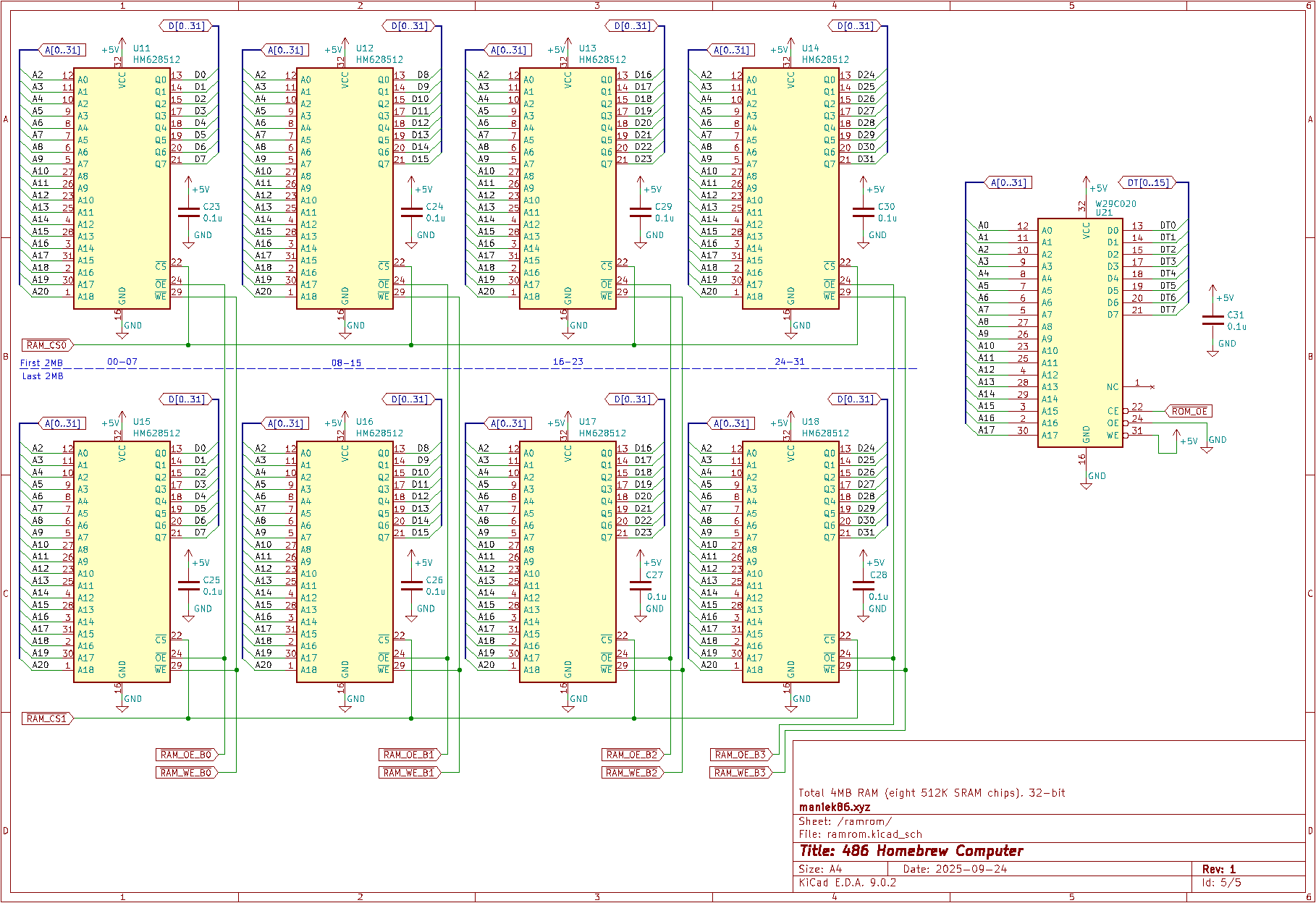
4 MB RAM:
There are 4 MB of RAM, organized into two banks of four 512 KB SRAM chips each. Considering my small budget, I researched cheap SRAM chips and found HM628512. I bought ten of them from AliExpress for about 35 PLN (~9.60 USD in December 2025) (The chips came relabeled - I will talk about this later). One issue with this chip is that it is slow: 55 or 70 ns. I think that's because this SRAM is designed for low power solutions. Apart from that, it's fine for our needs. The FPGA controls the WE, OE, and CS signals of the chips. I decided to use SRAM because it's easier to drive than DRAM. As for the experimental 486 homebrew, I think it's fine for now, but I plan to work on a memory controller that can use standard PC sticks - my idea is to try using 168-pin DIMM SDRAMs.
256 KB ROM:
I had a Winbond W29C020-90 in my spare parts bin. It's a 256 KB flash ROM. I think this is plenty for a 486 computer. Access to it is also controlled by the FPGA.
PCB Design
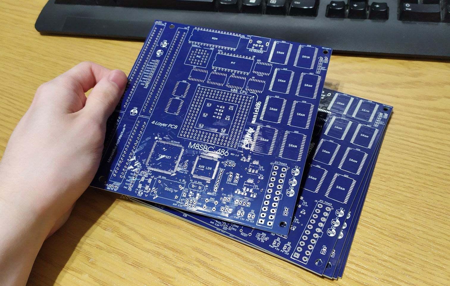
After looking at my finished schematic a few times, I decided to move on to the PCB editor. For the PCB parameters, I chose: 150*150 mm and four layers. I don't think it's a bad choice in terms of space and price. It's difficult to go smaller because the ISA connectors are about 14 cm long. Since I already had some parts available, I sketched the board layout on paper, planning where to place each large component so that it would be easy to trace and look good. By the way, this is the first 4-layer PCB I have designed!
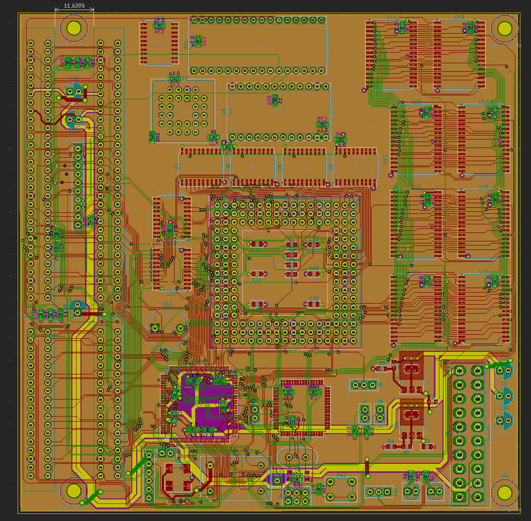
PCB during development
The design process was nothing special, just a lot of routing. I didn't consider the length or impedance of the traces. For this project, I don't plan to run it in a very edge case at more than 33 MHz. For the width of the signal traces, I went with 0.16 mm (~6 mils), and for the via size, I went with a 0.5 mm diameter and a 0.2 mm hole. I also decreased the default DRC margins a bit in KiCad. Everything is within the range of PCBWay's production capabilities. There are four layers: the two outer layers contain signaling, one internal layer is fully filled with ground and the second internal layer is 5V power with a few traces for 12V, -12V, 3.3V, and 2.5V. The entire routing process took about two weeks, but I was glad with the finished result.
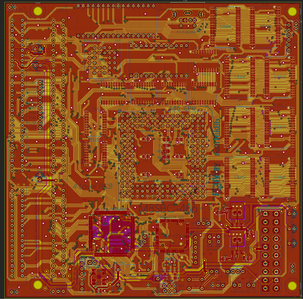
Finished PCB
After having the PCB done, I reviewed the entire project a few more times. Then, I went to the PCBWay website and ordered five PCBs. While I was waiting, I started working on the VHDL design for the FPGA. But that's a topic for the next part.
And this image shows more or less the architecture of this computer.
Last updated: 09/01/2026


![Validate my RSS feed [Valid RSS]](http://maniek86.xyz/cmsesus/uploads/image/valid-rss-rogers.png)
