

![[Valid RSS]](http://maniek86.xyz/cmsesus/uploads/image/valid-rss-rogers.png "Validate my RSS feed")

Homebrew 68000 computer with a PCI bus
[Back to the homebrew computers page]
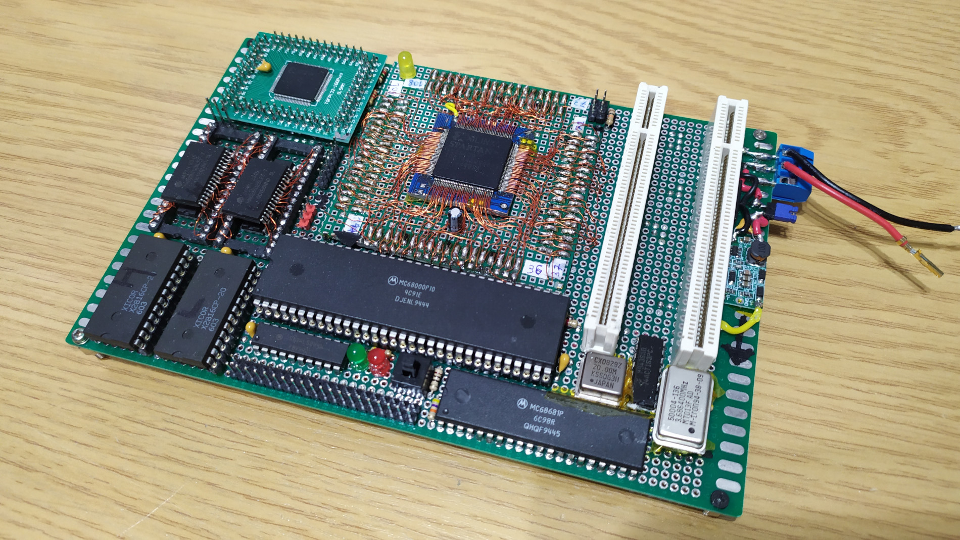
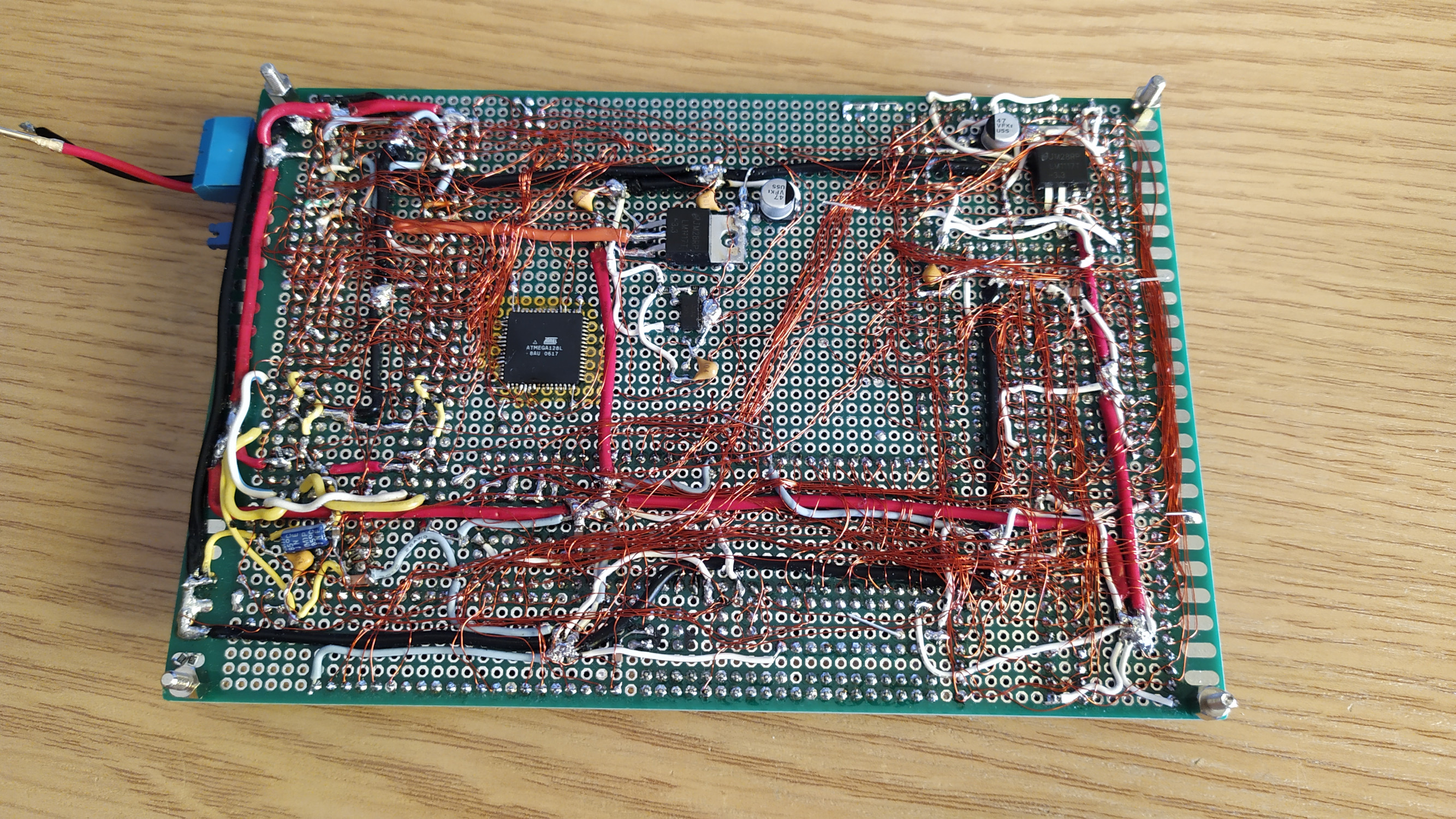
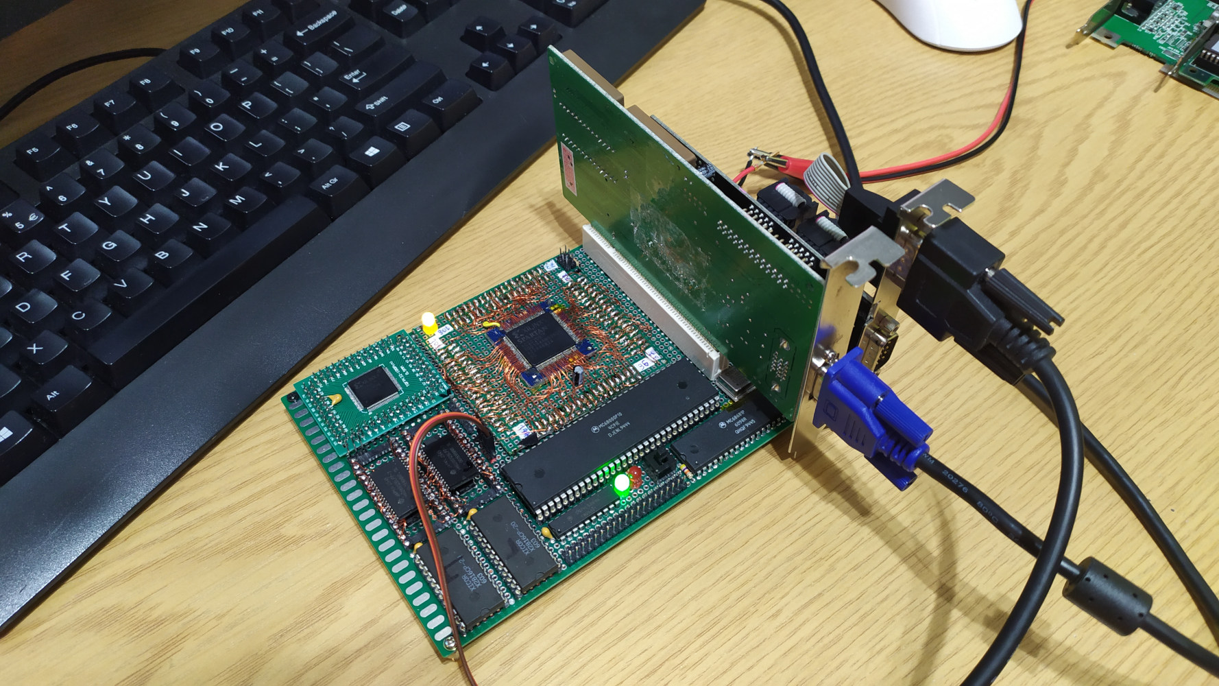
The finished result
Specs
- Motorola 68000 running at 10 MHz
- 1 MB of SRAM
- 4 KB of ROM
- MC68681P as UART, timer source and I/O
- Two 32-bit 5V PCI slots, interrupt capable, no bus mastering (no DMA). Xilinx Spartan II FPGA (XC2S100) as the PCI bridge.
- XC95144XL CPLD as glue logic
Current state: working and ready to go
Repository with code: https://github.com/maniekx86/m68k_pci
Schematic: http://maniek86.xyz/pliki2/m68k_pci/motorola_68000_pci.pdf
The PCI bus and the preceding experiment
During the late development of the M8SBC-486, I received suggestions of adding VLB (Vesa Local Bus) and PCI to it. At the time, I was more focused on the base board's functionality than on working on a new revision with new interfaces, so I dismissed the topic. While VLB is simple, as it is just a 486 bus exposed on a connector, PCI is not. PCI is a bus that requires a bridge to translate CPU cycles into its own cycles. It also allows for memory DMA via bus mastering. It's complicated on both the electrical and software levels.
However, since you are reading this, it means that I have finally become interested in the PCI bus. Around the middle of 2026, I got quite bored with the M8SBC-486 and wanted to do something more complicated. As of the time of writing, progress on the M8SBC-486 is slowing due to its hardware limitations. I finally became interested in PCI because of the many possibilities it offers. There are hundreds of cards that can extend the system in unique and cool ways. I started thinking about using the PCI bus in potential future projects.
Due to the complexity of PCI, it wasn't something that I could pick up in just two days by reading a few articles online. I needed to actually read about it. Reading the specifications directly is usually difficult, so I found a book titled "PCI System Architecture", released by Mindshare Inc. and started reading it since it's clearer.
Generally, I'm the type of person who enjoys learning through practical work rather than just reading theory and doing simulations. For example, my previous work with 486s introduced me to FPGAs quite well through direct experimentation. So, to learn about PCI, I wanted to do something practical, like building something physical that interfaces with the bus. I remembered that I had something interesting in storage related to this idea. They were old proprietary PCI cards with Xilinx Spartan 2 FPGAs on them - the XC2S100, which is also used in the M8SBC-486. I got them from my teacher at school as scrap (thanks again). You can find the full story about this on the 486 Homebrew page (History: My journey into FPGAs and CPLDs), so I'll skip it here.
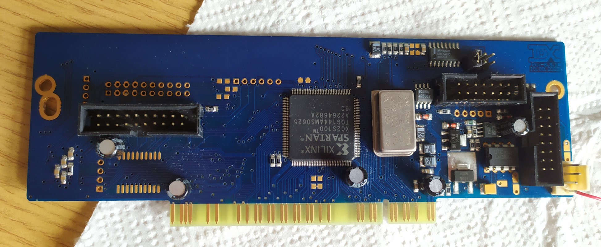
The important thing about these cards is that the FPGA connects directly to the PCI bus. This is great because it means I can work directly with it like I wanted. There was only one slight problem: these cards were proprietary and made only to order. There were no schematics, pinouts or anything. Solution? Reverse engineer them! I had more than one and some were already disassembled (like the FPGAs from two cards went to the M8SBC-486 boards). I used one of those as a reference. Using a hot air gun, I removed every remaining components on the board and I used a scanner to grab high quality scans of the PCB. The PCB is 2-layer, so I didn't have to use advanced techniques, such as grinding the board to access the inner layers. The task was to retrace it and create a schematic in the way.
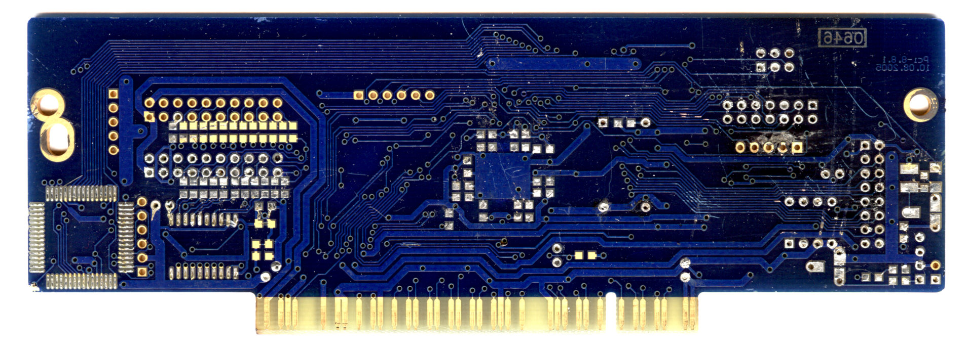
Tracing the board and creating the schematic took me about 3 to 4 days in total. The result was essentially a one to one recreation of the board in KiCad (well, almost one to one, as I later discovered some traces that I had forgotten to connect).
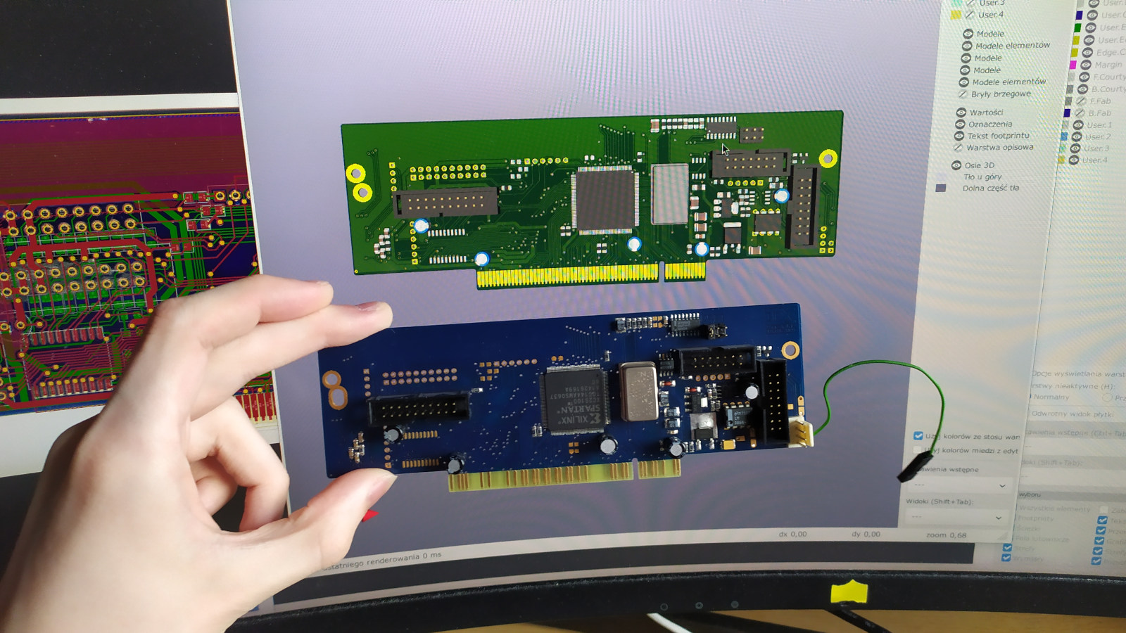
Now, with the recreated schematics of this card especially around the PCI section, I could say that I got a basic PCI dev board. One thing I like about the Xilinx Spartan 2 FPGAs I mentioned on the M8SBC-486 page is their 5V tolerance. This means I can use this card in 5V PCI environments.
Meanwhile, I was still reading the book about PCI. It was the only thing stopping me from creating something. I decided to read it until I knew how to make a basic PCI card. A card that could be detected in the system and accessed somehow. A few days later after more intense reading, I had understood enough to make a basic "target only" PCI card (a card that doesn't use DMA). So, I started writing some VHDL in Xilinx ISE.
With the help of the PCI System Architecture book and its timing diagrams, I created something that was detected by the system in just two days. This required me to implement the PCI protocol (bus signaling) and the PCI Configuration Space, which provides the system with information about the card (I will discuss the PCI bus in more detail later). The hardest part was the signaling. I had to correctly detect the configuration read command and respond with the correct data. A few hours later, I moved on to the configuration writes and BAR assignment, which I successfully implemented. I decided to give this experimental card a 64 byte memory BAR.
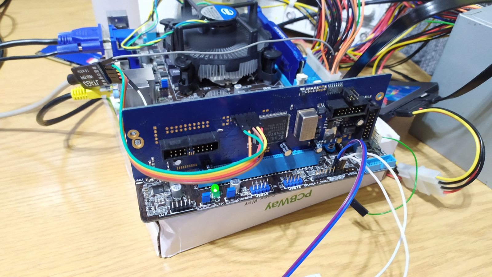
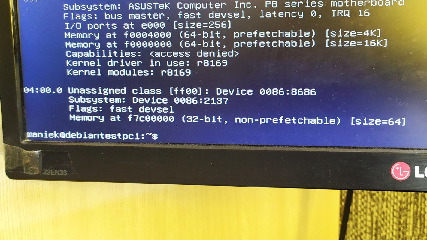
As time went on (the timescale here was literally hours), I finally got to the (final) point where the card:
- implemented configuration space reads and writes,
- implemented basic configuration space registers, thus allowing it to be detected,
- implemented internal 64-byte RAM and requested a BAR for it (a BAR allows the card to be assigned to the system's memory or I/O space),
- implemented reads and writes (the destination is the internal 64-byte RAM), including burst transactions,
- captured the first written byte and latched its contents to a few output pins, effectively making this first byte act as an output register.
And on top of that, I wrote a simple Linux test driver to bind to the card, test its internal memory and make an LED connected to one of the output pins blink.
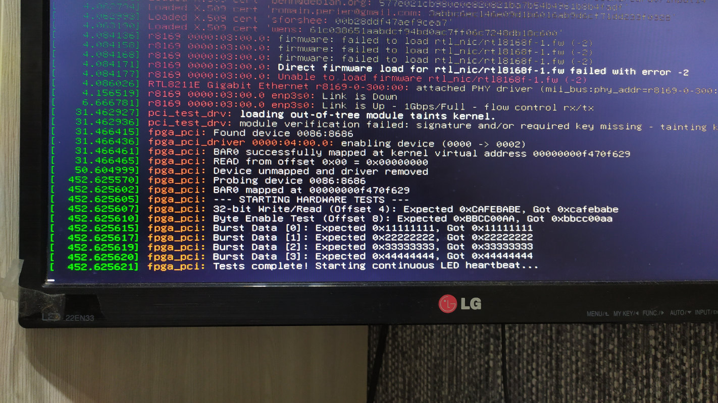
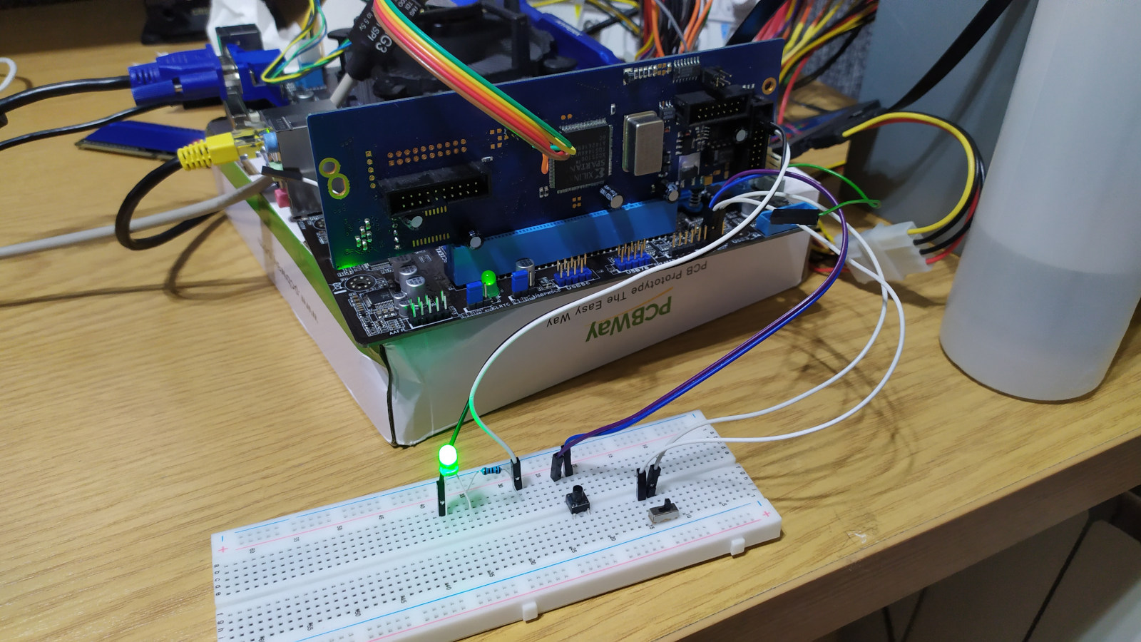
Ultimately, it was my first practical experience with the PCI bus. Even when I was working on hobby x86 operating systems back in 2023-24, I never worked with it. I was proud to finally understand the basics of the PCI bus.
How the PCI bus works
Before I continue with the main topic, I would like to briefly explain how the PCI bus works and why its implementation can be challenging.
Introduction
Most previous computer buses were simply connected directly to the CPU bus (for example ISA). Such a solution came with problems like potential device conflicts, the need for manual resource configuration (as opposed to auto detection), pin count (a 32-bit address bus plus a 32-bit data bus would require a minimum of 64 pins, not including power, control, DMA, interrupts, etc.), signalling (the ISA bus could officially run at a maximum of 8.33 MHz) and more. This became problematic in standard x86 PCs when they shifted to 32-bits (386 and 486) and increased in speed. Attempts were made to solve this problem by extending the ISA bus further. Standards such as EISA and VESA Local Bus (VLB) emerged, but they were unsuccessful in the long term. EISA had high manufacturing costs due to its special dual-layered slots and its low clock speeds derived from the ISA (8.33 MHz). The VESA Local Bus was essentially a 486 bus exposed on a slot, which made it difficult to implement in future CPUs. This is why Intel started developing the PCI bus to address these issues.
Although the PCI bus was initially introduced in x86 PCs, it was later adopted by computers based on other architectures too. Below is a list of its major features:
- Processor independence: unlike previously mentioned buses, components designed for the PCI bus are PCI-specific.
- Compact, efficient design - The basic bus is 32-bit. Data and address pins are multiplexed (AD signals). The connectors are small with only 124 pins.
- Speed - By definition, a basic 32-bit PCI bus runs at 33 MHz and can theoretically transfer data at a rate of 132 MB/s. This doubles to 264 MB/s when using the 64-bit extension and quadruples to 528 MB/s when the bus is run at 66 MHz (which it can do in some cases).
- Burst read and writes - As I mentioned, the data and address pins are multiplexed and the maximum speed of a basic 32-bit 33 MHz PCI bus is 132 MB/s. You might think that this speed would not be possible in such an implementation (two cycles for transfer: first address, then data). However, the PCI bus can perform burst transactions. Basically, after the device that accesses the bus presents the address on the 32 AD pins, the transaction doesn't have to end when it's time for the data on the pins. The accessing device, called the "initiator", can transfer more data without ending the cycle during the next clock cycles without presenting a new address. The device being read from or written to, called the "target", must internally track the increasing address with each data phase. Not every device has to support this, but the specification fully describes burst reads and writes.
Signaling
First, I would like to mention that the PCI bus uses a technique called reflected-wave switching. This is a signalling technique that uses the reflections of signals that are usually unwanted in data transmission to its advantage. This reduces the cost of a system board, because termination resistors are not needed. Although, this does require careful design of the board and signal drivers to meet constraints. I won't discuss this in detail here, since this homebrew computer runs the PCI clock at less than 33 MHz, so signal quality is not such a big problem.
Regarding the clock, the PCI bus runs at 33 MHz by default, but it can also be slowed down or stopped completely. The specification says this is for energy saving. Generally, PCI can operate at speeds as low as the kHz range! In PCI, everything is synchronous to the rising edge of the clock.
The PCI standard defines 5V and 3.3V signalling environments. This is achieved through connector keying, with 5V and 3.3V PCI slots and cards. There is just one exception to this: universal PCI cards. These can work in both 5V and 3.3V slots. The used standard depends on the system and card.
PCI is a local bus. It can operate independently of the CPU. It supports DMA via bus mastering. In essence, any PCI device can request access to the bus, after which a special arbiter grants it. It then takes control of the signals and becomes the "initiator". During this time, the device can access system memory or even other PCI devices on the bus. The host bridge, which connects the CPU to the PCI bus, is an example of a PCI bus master.
To reduce the number of pins required, PCI multiplexes the address and data pins (AD) as well as the command and byte enable pins (C/BE#). Unlike other older buses that are connected directly to the CPU, where the CPU simply activates the write or read signals and the cards respond to them, the PCI bus requires a "handshake". Each transaction starts, moves and ends with a condition.
An example of a PCI burst write transaction is shown below.
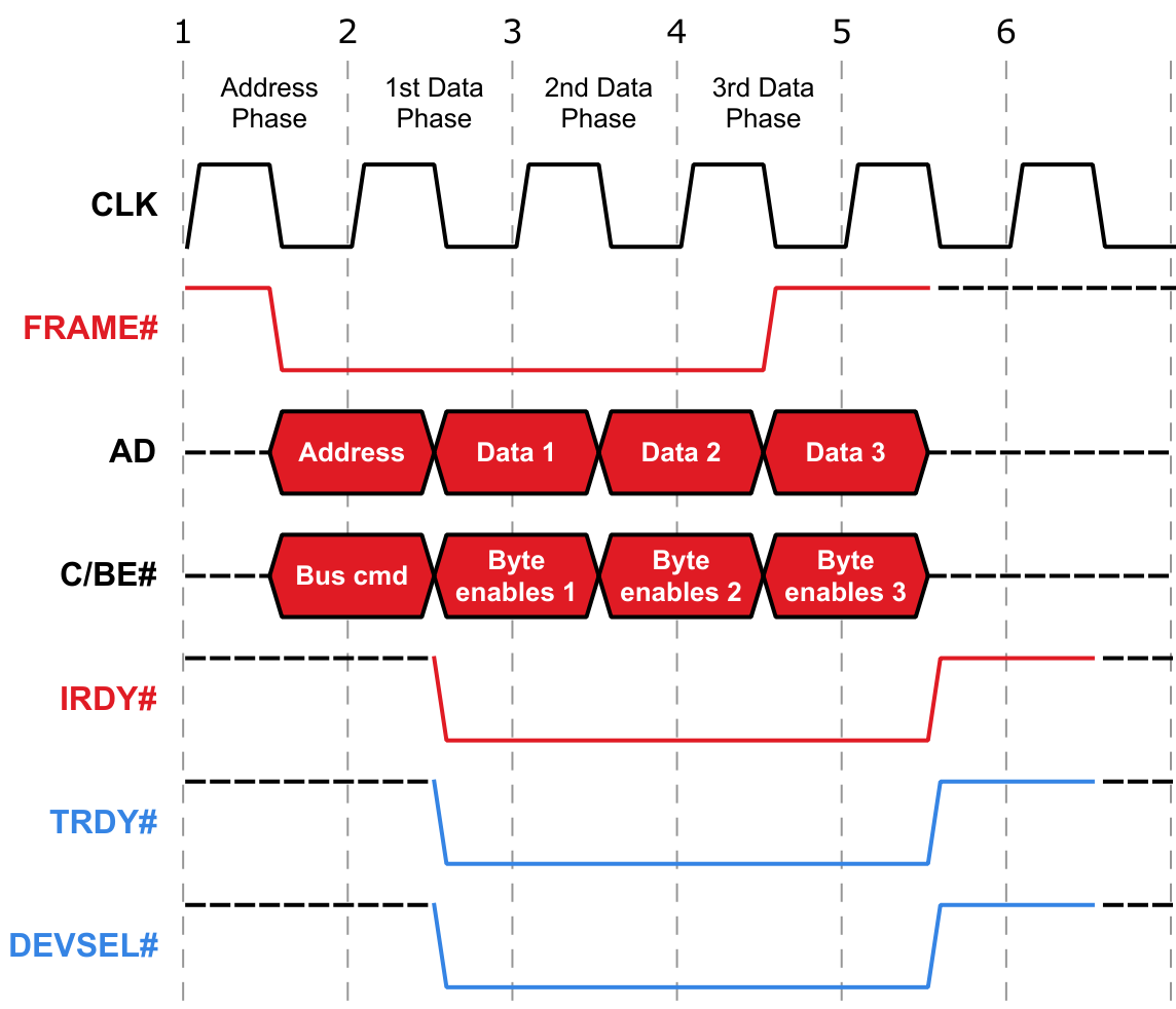
Signals:
- CLK - The clock to which signals are synchronized on the rising edge.
- FRAME# - Active low; this signal tells the entire bus that a transaction is beginning. This signal is pulled high by a resistor on the bus to prevent it from floating.
- AD - Multiplexed address and data bus.
- C/BE# - Multiplexed command and byte enable bus. At the start of a transaction, it indicates a command; during the data phases, it indicates which bytes are to be transferred on the 32-bit AD bus.
- IRDY# - Active low initiator ready signal, driven by the device that starts the transaction (initiator). This indicates that the initiator is ready to send the data. This signal is pulled high by a resistor on the bus to prevent it from floating.
- TRDY# - Active low; target ready; driven by the targeted device (target). It indicates that the target is ready to accept the data. This signal is pulled high by a resistor on the bus to prevent it from floating.
- DEVSEL# - Active low device select, driven by the targeted device. It indicates that the device has successfully decoded the address and that it is within its range. It should only be driven by one target device. This signal is pulled high by a resistor on the bus to prevent it from floating.
This example transaction involves the transfer of three packets of data without any wait states. The red signals are driven by the initiator and the blue signals are driven by the target.
Clock cycles:
- The initiator places the address on the address bus and the command on the C/BE# bus, while lowering the FRAME# signal. The command that it puts on the command bus is a memory write. This marks the start of a transaction.
- All PCI devices on the bus latch the address and check whether it falls within their range. If one of the devices does so, it starts outputting a low state on the DEVSEL# pin. Meanwhile, the initiator starts driving the first data and byte enables assuming it is ready instantly (it drives the IRDY# signal low). If not, the target has to wait until the initiator drives it low before it can latch any data. The initiator can also wait for the target by driving the TRDY# high instead of low. The condition for data transfer is for both the IRDY# and TRDY# signals to be low. In this diagram, both signals go low instantly, meaning that the target and initiator are ready. We can also tell that this data transfer is going to be longer than one item. This is because the FRAME# signal has not gone high. If it had, that would have meant that the next transaction would be the last one.
- All IRDY#, TRDY# and DEVLSEL# are low. The initiator knows that the device has been addressed properly (DEVSEL#). As the ready signals are all low, the first data item is transferred. As FRAME# is still low, the initiator wants to send more data. The target must increase the address that it latched on to at the beginning internally.
- The second data item is transferred. The initiator finally drives FRAME# high, meaning the next data item will be the last one.
- The IRDY# and TRDY# signals are low, so the final third data item is transferred. Both devices then drive the control signals high. As the frame was driven high one clock cycle earlier, it can now be released (raising it before releasing speeds up the process of pulling the line up to the high state ahead of the pulling resistor).
- All signals are released. The same quick pulling by driving applies to the other signals, so they are released in this cycle. The PCI bus is now free.
There might be a situation in which none of the devices lower the DEVSEL#. This means that the address is not covered by any of the cards. This results in an error called "Master Abort", which the operating system should handle. Additionally, there may be situations in which the target device does not support burst cycles. The target can abort the transaction by lowering a special signal named STOP#. One data item is transferred and then the transaction ends. To transfer more data, the initiator must repeat the cycle.
Read transactions are similar to this one. The only difference is that there is one enforced wait state after the address phase. This prevents situations in which two devices try to drive the AD bus at the same time when the directions switch. The initiator writes the address onto the AD bus, releases it, waits one cycle and starts a normal data transaction.
I skipped a lot of information, including more explanations of wait states, timeouts (e.g., master aborts), signals (e.g., STOP#), arbitration and more to simplify this brief introduction to the PCI bus. If you want to know more, I recommend reading some literature about it.
PCI software architecture
From the perspective of software, the PCI is divided into three different accessible spaces:
- Configuration space: Every card must have a hidden 256-byte configuration space. This space identifies the card and informs the system of its capabilities and requirements. This includes Base Address Registers (BARs). The BARs tell the system what kind of space (memory or I/O) the card requires and how much of it. Cards can request up to 6 different BAR blocks. These registers can also be written to and are used to map the card to the system space. After mapping the card with the BAR and enabling the correct bits in the control register (which resides in the configuration space), the card starts responding to the set address.
- Memory space: Used for large data blocks, such as video memory.
- I/O space: A x86 legacy concept retained by PCI. It is used for the usual control registers.
These spaces are accessed by the C/BE# bus value (command) in the first cycle. It can be: Configuration read/write, memory read/write or I/O read/write. For the configuration space, the desired card is selected by a special signal - IDSEL, which is unique to each PCI slot.
Endianness
The PCI bus is designed to be little-endian. The value 0xAABBCCDD is stored in memory as follows:
- offset +0 (AD [7:0]): 0xDD,
- offset +1: 0xCC,
- offset +2: 0xBB,
- offset +3 (AD [31:24]): 0xAA.
However, on big-endian CPUs, such as the Motorola 68000, the same value stored in memory looks like this:
- offset +0: 0xAA,
- offset +1: 0xBB,
- offset +2: 0xCC,
- offset +3: 0xDD.
This becomes problematic when trying to interface the PCI bus with such CPUs. To correctly address bytes or read 16- or 32-bit registers, we need to swap bytes in software or hardware.
There are two techniques we can use for that. We can either preserve the value or the address. The first technique is essentially swapping bytes on the data bus in hardware, ensuring that the 16- or 32-bit number remains unchanged. If the code requests 0xDEADBEEF, the CPU receives 0xDEADBEEF exactly. The issue with this solution is that accessing data in smaller sizes is not straightforward (addressing causes bytes to get swapped). In the second method, we cross the bus so that byte 0 goes to address 0, byte 1 goes to address 1 and so on. We don't care if larger values get scrambled, because we want to preserve the accessed address.
So, value preserving is used when reading or writing a big 32-bit hardware register (like a BAR register) and location preserving is used when writing an array of sequential bytes, like a C string (char*) or a continuous buffer of VGA pixels. With this second method, you get the array to land left to right, exactly as you typed it. Keep this in mind, as I used both methods in the project.
Interrupts and functions
One last thing I would like to mention is PCI interrupts. Each PCI slot has 4 interrupt pins: INTA#, INTB#, INTC# and INTD#. Why four? The PCI specifications allow one PCI device to behave like multiple devices, up to eight. These "subdevices" are called PCI functions. Each function has its own configuration space and registers. Multiple interrupt lines allow interrupts to be spread out onto different potential CPU interrupt lines. Additionally, single-function devices must use the first line INTA#. These interrupt pins are simple: they are standard active-low interrupt pins. They are typically shared; for example, each INTx# pin is connected to other INTx# pins on the board and routed directly to a CPU interrupt line. Shared interrupts are common in PCI.
Once again, I skipped a lot of information about PCI. I explained the basics; probably enough to understand the challenges of implementation. You can find sources and more information here:
- Wikipedia: Peripheral Component Interconnect,
- OSDev.org: PCI, PCI Local Bus Signals, PCI Local Bus Commands.
The idea
After this rather extended introduction, I will now move on to the main topic of this page: the Motorola 68000 homebrew computer with a PCI bus. The idea for this computer actually came to me by coincidence. I received a lot of electronics scrap from my friend Shadowdestroyer777 (huge thanks!). This included an industrial board with a Motorola 68000 CPU, as well as two older broken motherboards (Socket 7 era) for parts. I desoldered the components from the industrial board and one of the broken boards, including the expansion slots, socket, etc. (This was shortly after I had finished working on the experimental FPGA PCI card). The parts from all this work ended up on my desk. One evening, while looking at the desoldered PCI slots, the Motorola 68000 CPU and a prototype board that I had also bought a short time ago, I suddenly thought: "What if I built a 68000 homebrew with PCI on a prototype board?" - and that's how the idea was born.
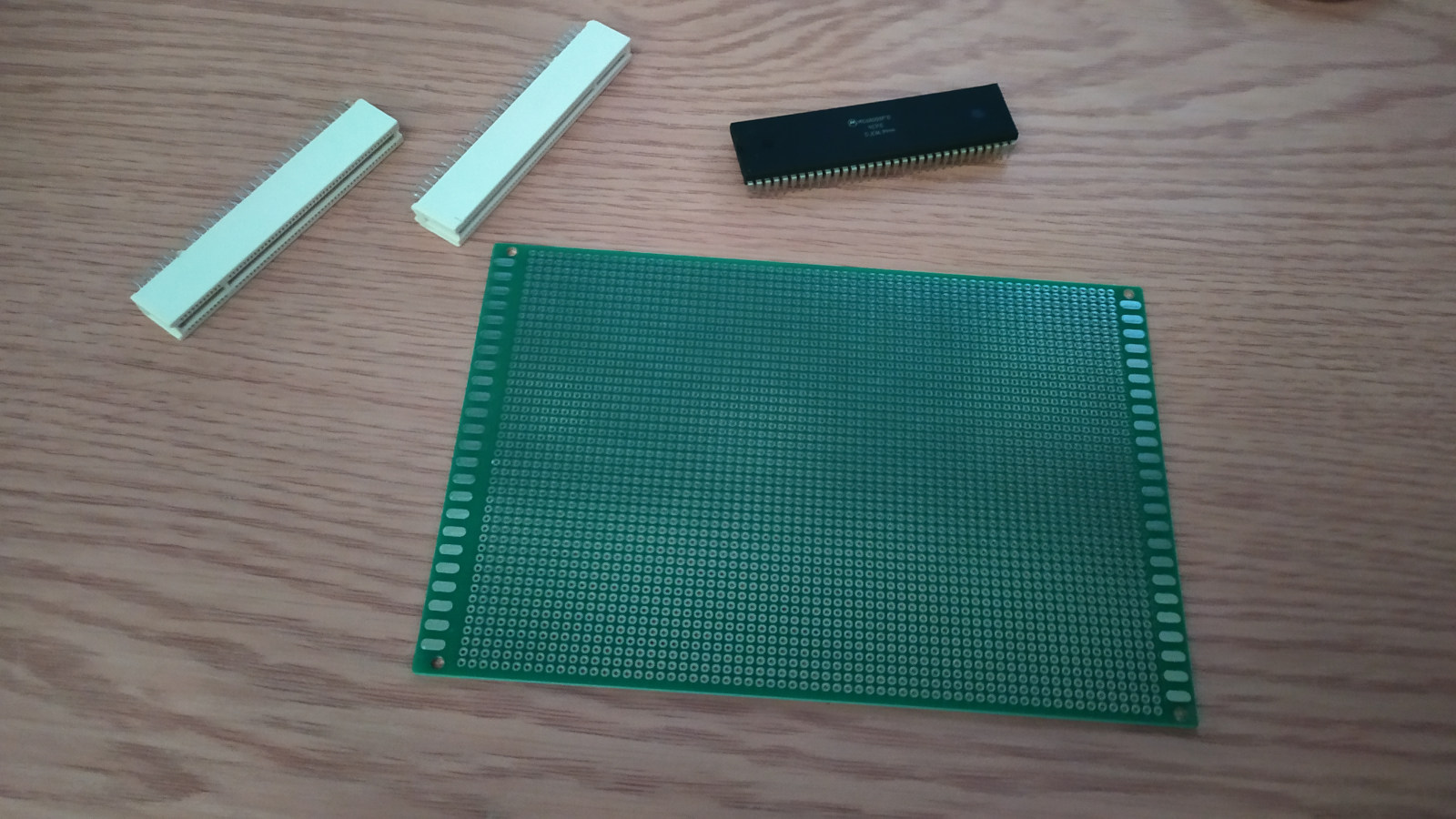
I took this photo literally when the idea struck!
The prototype board I had was 12x18 cm. At this point, I didn't know which other parts I would use, so I started checking my drawers to see what I had. After searching, checking and selecting, I decided to use the following parts:
- MC68000P10 - a Motorola 68000 CPU, 10 MHz max, from the mentioned scrap lot.
- XC95144XL CPLD for the glue logic - I still had a few of these left over from previous projects.
- Two HM628512 SRAMs, 512 KB each - more leftovers, this time from the M8SBC-486.
- Two Xicor X2816C EEPROMs, 2 KB each - for the software.
- MC68681P DUART - the same UART chip that I used in my previous Motorola 68000 homebrew project. This time, it will also be used for UART and timing (it has a built-in timer).
- 74245 and 74244 buffers - For the IDE disk interface.
- 7405 open collector inverter - For reset.
- Two PCI slots in a 5V configuration with a Xilinx Spartan 2 FPGA (XC2S100) as the host bridge - the main goal of this project!
- ATMega128 - used solely for loading the FPGA bitstream (added later).
I also had a 10 MHz crystal oscillator, which I decided to use as the main clock for everything, including the PCI bus. The idea was to run the PCI bus at the same frequency as the CPU to make it easier to design the logic (FPGA). As I mentioned in the chapter about PCI, the bus is permitted to run at less than the standard 33 MHz. I can also say in advance that the oscillator I used turned out to be faulty. Ultimately, I had to replace it with a 20 MHz oscillator and squeeze in an extra 74163 (4-bit counter) to divide the frequency by two (I didn't have any other 10 MHz oscillators).
There were few challenges because of the parts I had selected:
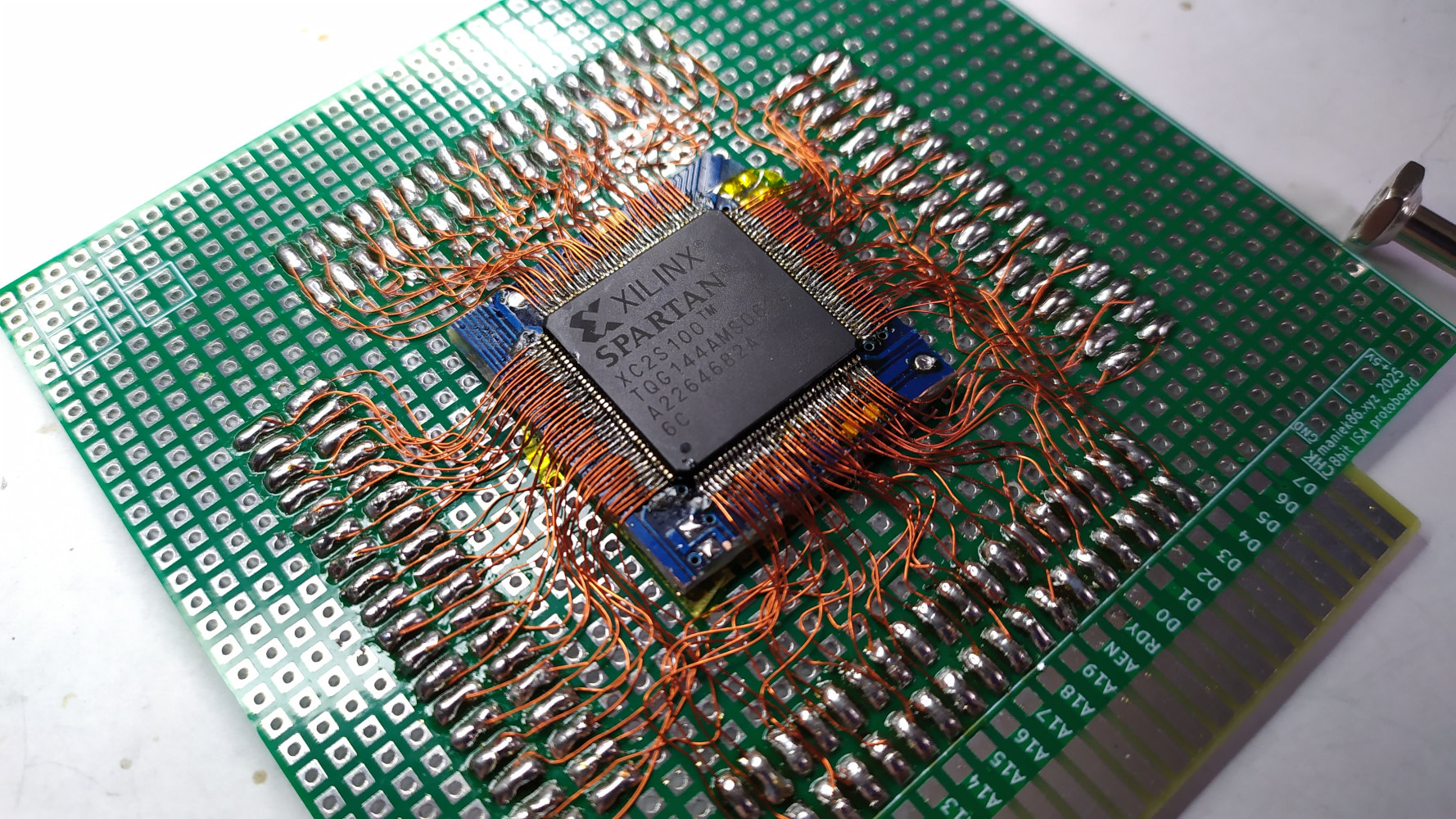
- Mounting the SMD parts: I decided to use some SMD parts. For example, the XC95144XL CPLD is in a QFP-100 package. Fortunately, I had a breakout board for it. However, I didn't have adapters for other parts, such as the SRAM chips or the Spartan 2 FPGA (QFP-144). To save money, I decided to adapt these parts myself. You might think adapting a 144 pin QFP chip manually is crazy, but I did it some time ago. While experimenting with the XC2S100 FPGA before designing the M8SBC-486 board (which uses it), I decided to mount that FPGA on a prototype board to check in practice its requirements. I manually soldered 144 thin enameled wires to the FPGA, which took me about three days (if I remember correctly). I ended up using an empty ISA prototype board (it was the only prototype PCB I had at the time - I didn't even use the ISA part - and I still have a few of those. Thanks PCBWay!). After I had finished that experiment, I left the board in my drawer, unused. For this project, I had the insane idea of using an angle grinder to extract the chip from the ISA board. The photo before cutting is below. Other examples are the SRAM chips. These are in a SOP package and can easily be adapted to a DIP by soldering a socket onto the board and connecting the chips to it using enameled wire
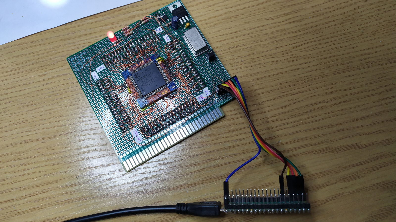
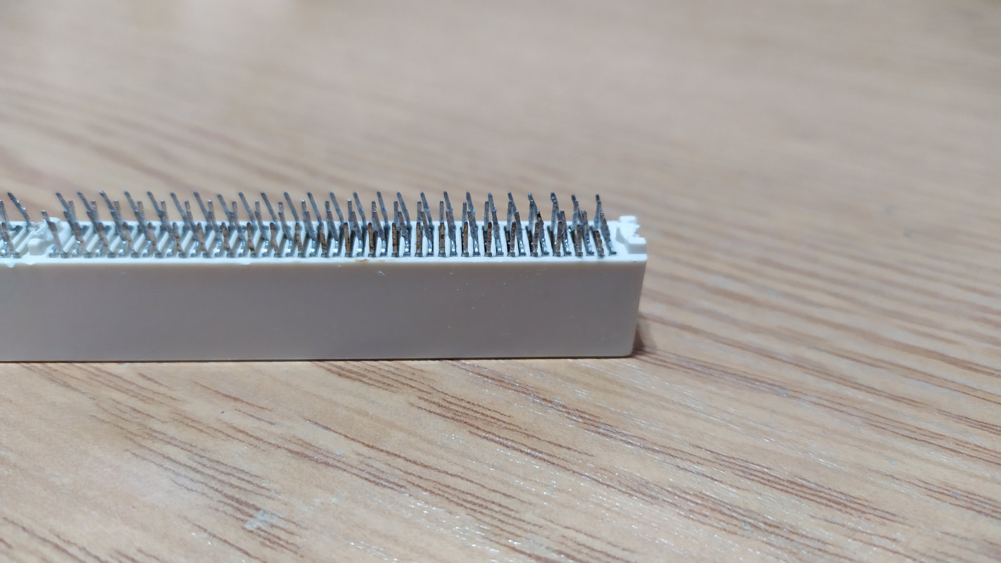
- PCI slots mounting: standard PCI slots quite use standard 2.54 mm spacing, however the alternating pins are shifted by 1.27 mm. My solution to that problem was to bent alternating pins to match 2.54mm spacing. This allowed me pretty easily to put in the PCI slots into the prototype board. Photo of this solution below.
- Space constraints: I thought I could easily fit everything on an 18x12 cm prototype board, but I was wrong. It took me some time to organize a reasonable layout. Everything is really tight! Some elements ended up on the back of the board, like some SMD components.
To connect all the components, I decided to use the same enamelled wire that I used for the 486 homebrew computer on a prototype board project. To prevent issues this time, I decided to inspect every wire for potential cracks in the insulation before soldering. (Quick story: that 486 computer doesn't work anymore because I didn't check the enameled wires, which probably have cracks in the insulation and are shorting).
With the chosen components, there were other things I had to consider. The first thing was power. The whole board runs on 5V logic and power; however, the XC95144XL CPLD requires a core voltage of 3.3V and the Spartan 2 FPGA requires 2.5V. The PCI also requires 3.3V power (regardless of whether it's 5V or 3.3V version, both rails must be supplied). I could have used a dual power supply, but I wanted to power this board with just 5V. I therefore decided to use LM1117 regulators that I had in storage. Two 3.3V ones and one adjustable one. I gave the CPLD its own 3.3V regulator and used the other 3.3V regulator for the FPGA (I/O) and PCI. I configured the adjustable regulator to 2.5V and used it for the FPGA's core voltage.
Regarding the overall system design: I reused many aspects of my previous 68000 homebrew computer, such as the reset circuit, the DUART and more. A significant difference between this project and the last one is the use of interrupts. Previously, I skipped interrupts to simplify the design, but this time with a CPLD acting as the system logic, I can reflash it with new logic as required, eliminating potential bugs and simplifying the design process overall. I began working on the CPLD design (in VHDL) after I had finished soldering everything necessary to get the CPU to run code (power, address/data buses and essential control lines). This time while working on the board, I also created a schematic so that I would not get lost in the mess of wires.
With that in place, I began soldering the board.
Soldering and initial tests
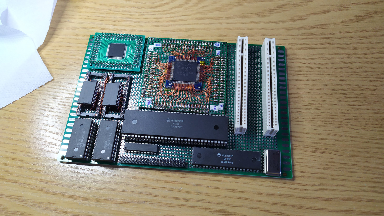
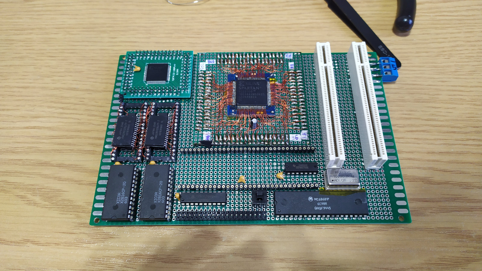
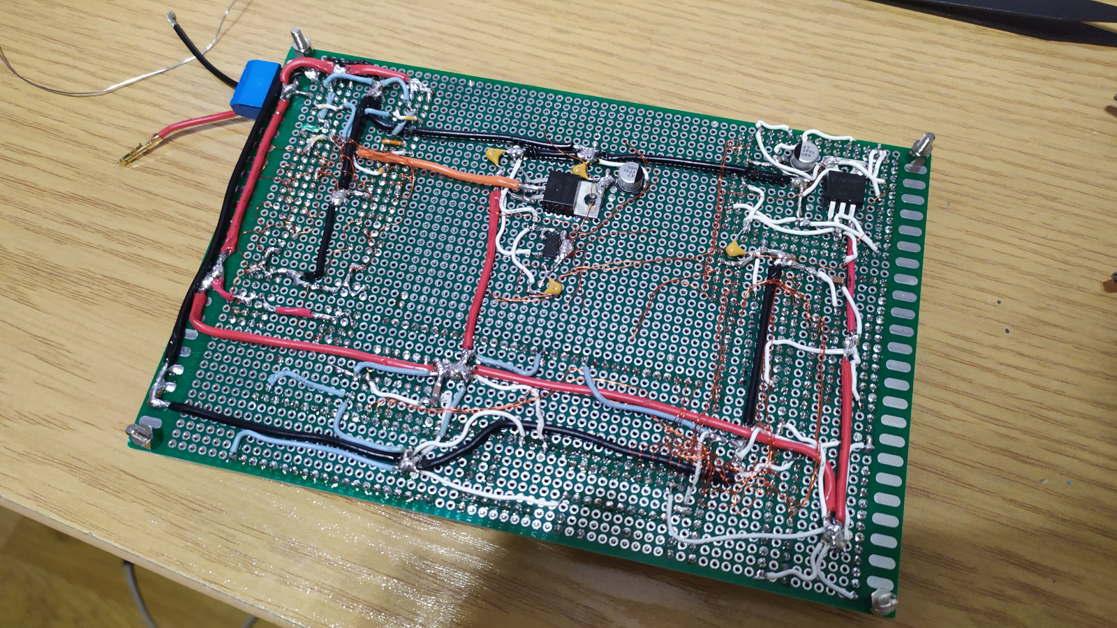
The first things I connected were the power wires and the power regulators. I added some capacitors to smooth out the power rails.
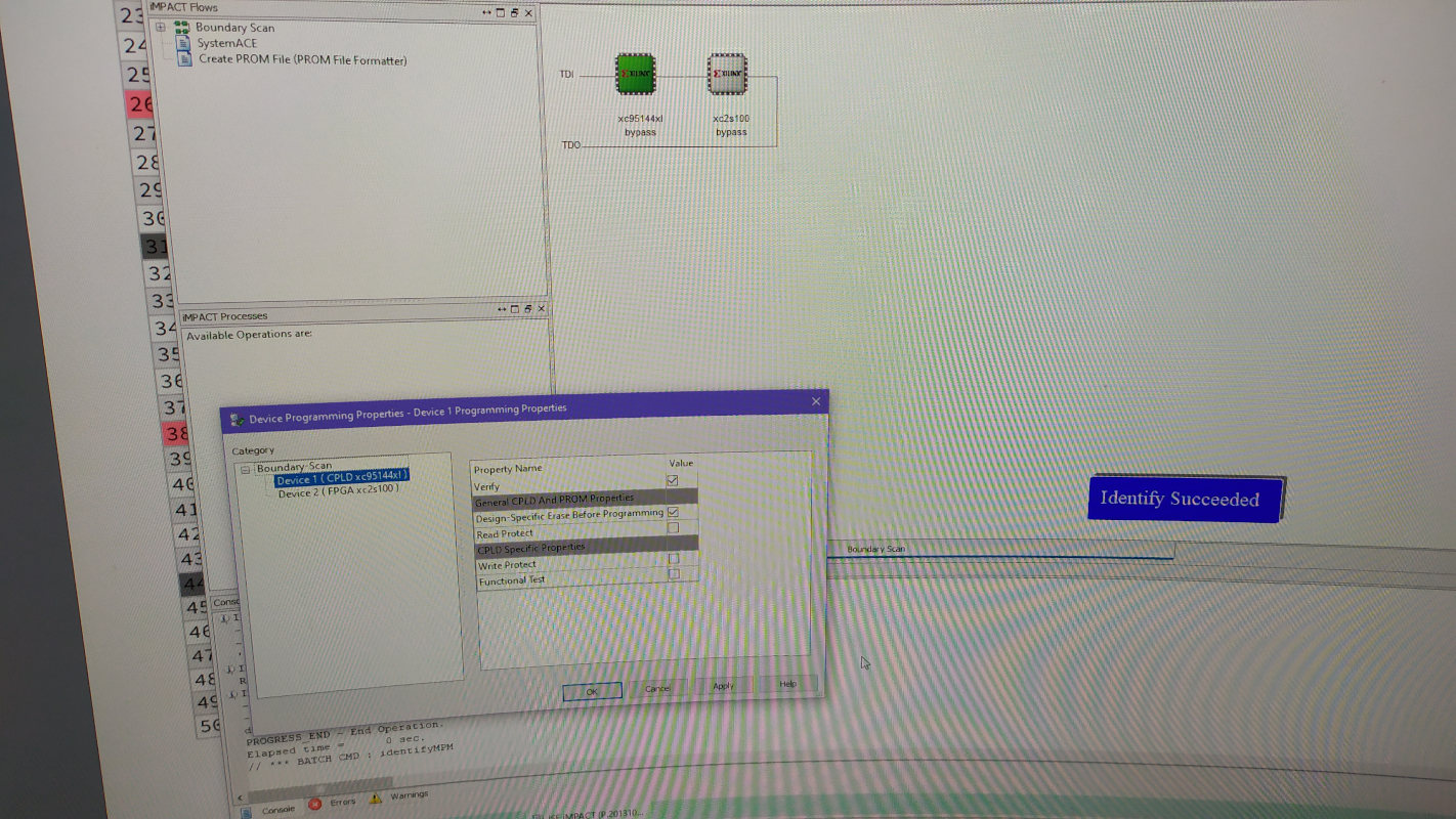
To test that the CPLD and FPGA were working, I soldered a JTAG connector. I connected the CPLD and the FPGA in a daisy chain. Both devices were detected on the first try!
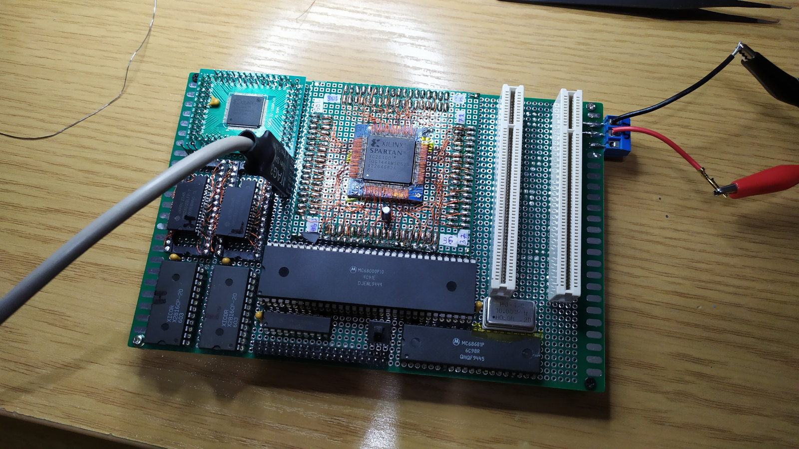
After that, I finished soldering the CPU to the RAM, ROM and CPLD. It was then that I discovered the 10 MHz crystal oscillator was broken. I quickly replaced it with the previously mentioned 20 MHz crystal and 74163, then started working on the first version of the CPLD logic to get the CPU to execute its first instructions on this board.
This homebrew has a pretty straightforward memory map:
- 0x000000 - 0x0FFFFF: RAM (1 MB),
- 0x100000 - 0x100FFF: ROM (4 KB),
- 0x200000 - 0x200FFF: DUART,
- 0x300000 - 0x300FFF: IDE,
- 0x800000 - 0xFFFFFF: PCI (8 MB).
Since the Motorola 68000 fetches the startup vector from the beginning of its memory space, I had to write a simple overlay feature that alters the address decoder's behavior. After the reset, the RAM is inaccessible and the ROM takes its place. This ensures that the startup vector is fetched from the ROM. When the CPLD detects access to the ROM at its actual address, it toggles off the overlay, making the RAM accessible.
    -- ROM overlay over RAM trick to allow start vectors to be at 0x000000
    -- After reset detection, we turn on ROM_BYPASS to overlay ROM over RAM
    -- As soon as we detect ROM being accessed, we turn off the ROM_BYPASS to allow RAM to be accessed
    PROCESS(CLK, RESET_n, ADDR)
        VARIABLE ADDR_msb : STD_LOGIC_VECTOR(23 DOWNTO 20);
    BEGIN
        ADDR_msb := ADDR(23 DOWNTO 20);

        IF RESET_n = '0' THEN
            ROM_BYPASS <= '1';
        ELSE
            IF RISING_EDGE(CLK) THEN
                IF ADDR_msb /= X"0" AND AS_n = '0' THEN -- AS must be low so we toggle only on valid cycles
                    ROM_BYPASS <= '0';
                END IF;
            END IF;
        END IF; -- RESET_n = '0'
    END PROCESS;
The ROM_BYPASS signal in the snippet above tells the address decoder to decode the ROM instead of the RAM when it is 1.
Apart from creating address decoding, I also had to write the RAM OE/WE signal generation, CS assertion logic and DTACK logic to make the initial logic work properly with the CPU. I tied the outputs of things like the interrupt logic and IDE signal generation to static values because they were not yet designed and in use. I flashed the initial design to the CPLD and I noticed the CPU attempting to fetch data from the ROM! I quickly wrote a simple infinite jump in assembly and compiled it using the ASMX assembler. Then, I flashed it to the EEPROMs and turned on the homebrew. It didn't work. I had swapped the lower and upper EEPROMs during the flash. Fortunately, after fixing this, it worked! I didn't make any mistakes soldering the mess of wires on the back.
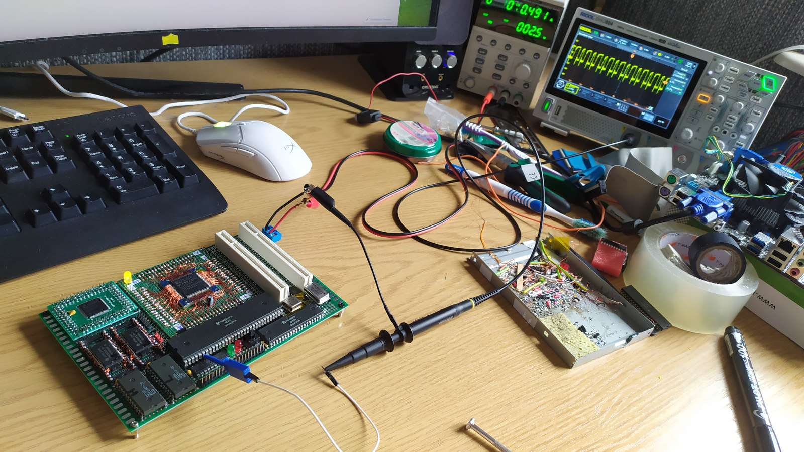
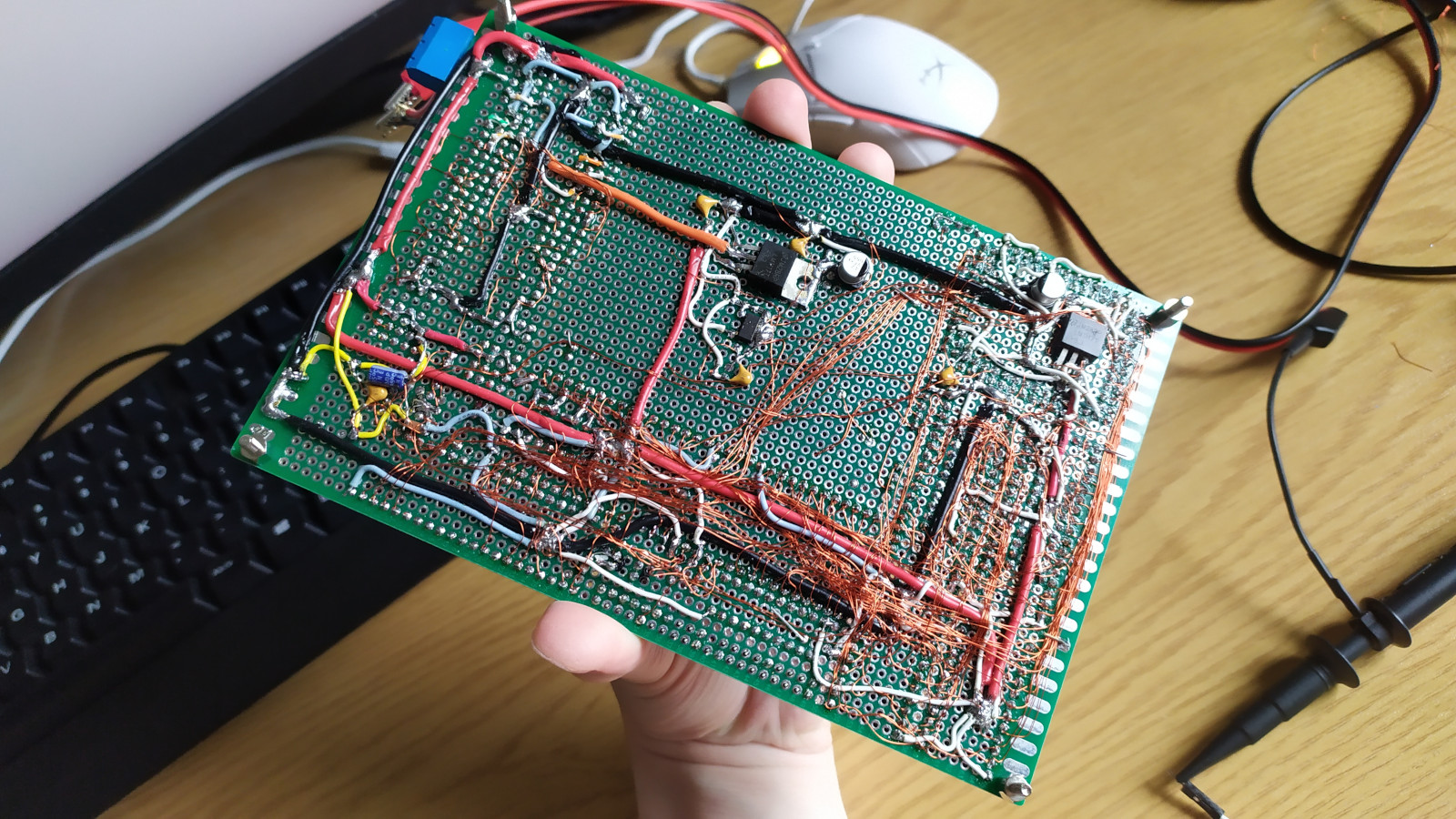
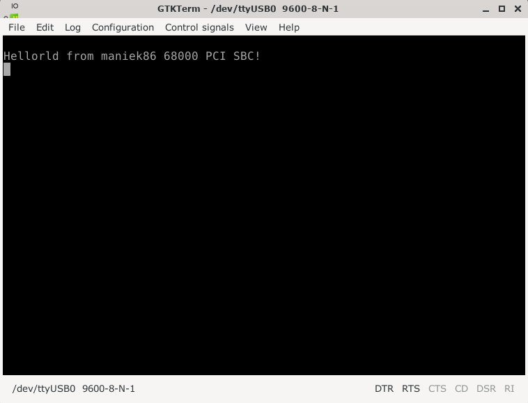
Before continuing further with soldering, I wrote a few simple assembly programs. I wrote a memory test to check if my addressing logic was working (which it was), as well as some DUART tests. I had some issues with the DUART because I had wired the R/W line incorrectly, which caused it to work randomly. It took me a while (about 4 hours) to discover this, as I suspected that I had wired something else incorrectly, like the DTACK/CS or that I had messed up the CPLD logic. But finally, after resolving that annoying issue, I saw the first characters on the terminal screen!
I connected an LED (the green one) to one of the MC68681P DUART's output pins. The blink demo was accomplished as well!
The C toolchain
I wanted to quickly get a C toolchain working on this computer because working with PCI in assembly would be very hard. One thing I like about the Motorola 68000 processor is that it has official GCC support. On my main Linux desktop (Debian 13 at the time of writing), the 68000 toolchain is present in the Debian repository. All I have to do is install gcc-m68k-linux-gnu and I have a compiler! In my opinion, it's great that a processor with a standard 2.54 mm spaced DIP package has full C capability.
The "linux-gnu" version of GCC has one important caveat: it's optimized for writing programs that run under Linux. I can't use any of the built-in libraries because they usually assume certain things. For example, standard Linux requires an MMU, so the included Debian toolchain defaults to newer processors like the 68020. This means its pre-built libgcc.a uses 32-bit math instructions that are invalid on an original 68000 processor. However, being aware of issues like this enables us to address them and use this version on bare metal. For instance, we can disable the default libraries from being included and provide a fixed version of the required routines.
In the current era of AI, I decided to use it to save time by creating a base build system for C. After entering the base system details, the AI helped me generate a Makefile, a linker script and a bootstrap assembly with an empty main entry in C code. It also quickly and properly wrote a replacement for libgcc.a. I don't like using AI for entire projects, but as a time-saving and verification tool, it's great.
All sources are available on the GitHub.
Interrupts
As I mentioned before, I skipped interrupts in my previous Motorola 68000 homebrew because I thought they were too complicated. However, working on the M8SBC-486 project showed me that's not true - especially on the 68000, which has three interrupt pins that allow it to recognize 6 maskable interrupts and 1 non-maskable interrupt without needing an external interrupt controller. With that in mind, I knew from the beginning that I wanted this new computer to use interrupts. In my design, these will handle DUART receives, DUART timer ticks, IDE interrupts and eventually even PCI interrupts. Getting this working physically was just a matter of soldering the IPL0-2, FC0-2 and VPA pins to the CPLD. Inside the CPLD, I wrote logic to decode the various external interrupt lines into the proper 3-bit combinations on the IPL pins, which tells the CPU exactly which interrupt is being triggered. When the CPU begins an interrupt acknowledge cycle, the CPLD detects this via the FC (Function Code) pins. The CPLD then asserts the VPA (Valid Peripheral Address) signal, which tells the CPU to use autovectoring. This simply means the processor determines the interrupt vector internally based on the value on the IPL pins, rather than expecting an external device to provide a vector on the data bus.
Here's a snippet of the final interrupt controller:
    -- Interrupts
    PROCESS(UART_IRQ_n, IDE_INTRQ, PCI_INT_S1_n, PCI_INT_S2_n, PCI_INT_EN)
    BEGIN
        IF UART_IRQ_n = '0' THEN
            IPL <= "011"; -- Level 4
        ELSIF IDE_INTRQ = '1' THEN
            IPL <= "100"; -- Level 3
        ELSIF (PCI_INT_S1_n = '0' AND PCI_INT_EN = '1') THEN
            IPL <= "101"; -- Level 2
        ELSIF (PCI_INT_S2_n = '0' AND PCI_INT_EN = '1') THEN
            IPL <= "110"; -- Level 1
        ELSE
            IPL <= "111"; -- Level 0: none
        END IF;
    END PROCESS;
As you can see, the VHDL IF/ELSIF structure inherently acts as a hardware priority encoder. By checking the DUART first, it receives the highest priority (Level 4), followed by the IDE interface (Level 3) and finally the PCI slots (Levels 2 and 1). This hierarchy dictates how the CPU handles simultaneous requests. If the IDE drive and the DUART both trigger an interrupt at the exact same time, the CPLD will output Level 4 to the IPL pins. The CPU will jump to the DUART's interrupt routine first and only after that interrupt is cleared by the software will the CPLD assert Level 3 for the pending IDE request.
In C code, interrupts were easy to support thanks to the built-in GCC interrupt attribute. After defining such a function, all I had to do was set its address in the correct entry of the Exception Vector Table (which is located within the first 1024 bytes of the address space and contains 256 entries).
Bootloader
With the CPU now working and executing actual C code and the DUART transmitting and receiving data using interrupts, I decided to write a bootloader for the first time in any of my projects. In previous projects, I had to constantly reflash ROMs and with the "two-chip architecture" (one chip for the lower byte and a second chip for the higher byte of the 16-bit data bus), reflashing two ROMs at once when an issue in the code occurs becomes tedious. I knew that I might need to make a lot of iterations to the code when working on the PCI, so I decided to write a bootloader this time.
My idea for the bootloader was to create something simple. The target program would be sent in 96 byte chunks (the uploader would send 96 bytes and then wait for a confirmation byte, which would act as a form of flow control). At the beginning of the upload process, the file size is sent so that the computer knows how much data to expect. As these 96 bytes are received, the buffered data is written to the target memory at 0x000400 (right after the Exception Vector Table). While receiving, the bootloader also calculates a checksum, which it then sends at the end to the uploader. This tells us if the upload was successful (when the expected checksum matches the received one). The uploader on the host side is written in the C. I also set the MC68681P baud rate to its official fastest setting: 38400. From my tests, 20 KB is uploaded in about 6 to 8 seconds.
The loaded program is another C program, but with different initialization code and a different linker script (as it runs in RAM in contrast to ROM). One issue with this approach is that the single serial port exposed on the board is occupied during upload. The MC68681P has two UART channels (which is why it's called DUART). I could have used the second channel, but due to a lack of space on the board, I chose to make the program wait for UART input before running. Essentially, it only initializes the DUART and interrupts and then waits for me to open the serial console and press any key. This way, I can see the text output!
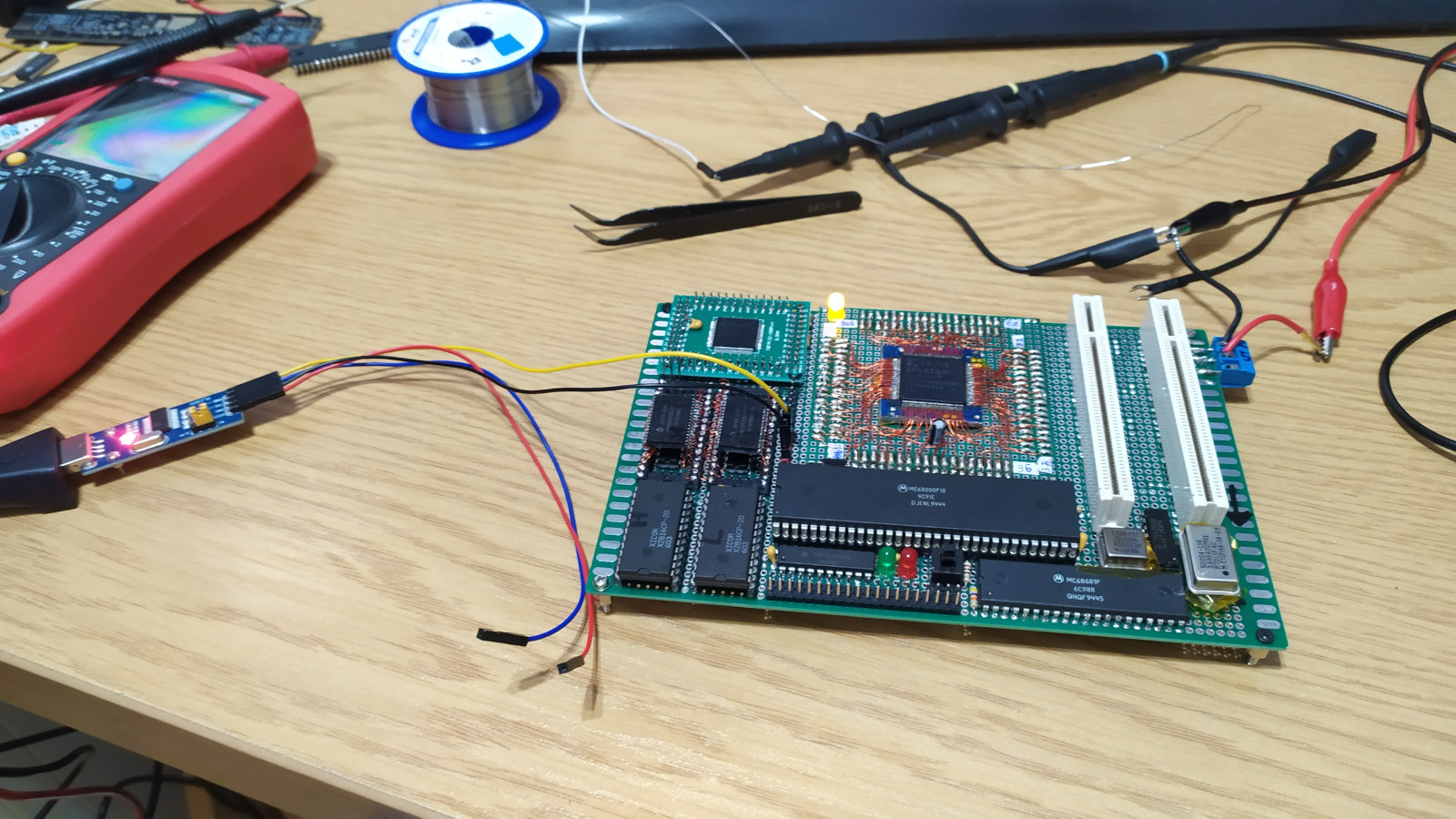
Implementing the PCI bus
FPGA-CPU interface
Once I had finished the base board and bootloader and ensured that everything was stable, I could finally move on to the PCI. This involved some more soldering. To avoid getting lost during soldering, I created a sheet showing which FPGA pins connected to what. This time, I optimized the pinout so that I would not have to solder very long wires (e.g. the CPU address lines were close to the CPU, while the PCI lines were close to the slots). As for the FPGA pin usage, I used almost every pin.
First thing I focused on was to solder the FPGA to the CPU, so I can try to design a interface for Motorola 68000 bus. This took me some time as I had to solder almost entire address bus, data bus and few control lines. With that done, I started working on initial logic design for the FPGA and it was quite difficult to do.
The Motorola 68000 bus is asynchronous, with the CPU sampling signals on both edges of the clock. I wanted my FPGA design to have only one clock domain with no clock division (with everything running at a ratio of 1:1). Due to the PCI, I chose to synchronize everything on the rising edge. The Motorola 68000 bus states are described in the datasheet as S0 to S7, with S0, S2, S4 and S6 occurring on the rising edge and the rest on the falling edge. Memory access starts on S0, but the FPGA cannot detect this until S4. This is because the address strobe signal goes low on S2. Additionally, if we want a zero-waitstate write or read, we must determine this now because the Motorola 68000 samples the DTACK (data acknowledge, which is basically equivalent to data ready) signal at the end of the S4 cycle, which occurs less than half a clock cycle later (because of the asynchronous bus)!
Below are diagrams of Motorola 68000 bus zero wait state reads and writes. The first image shows a read and the second shows a write.
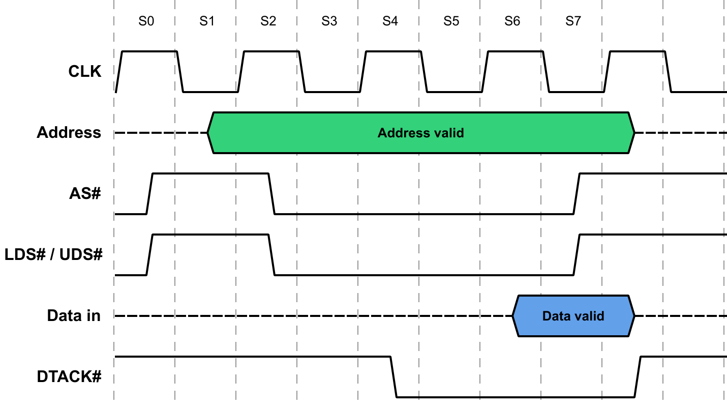
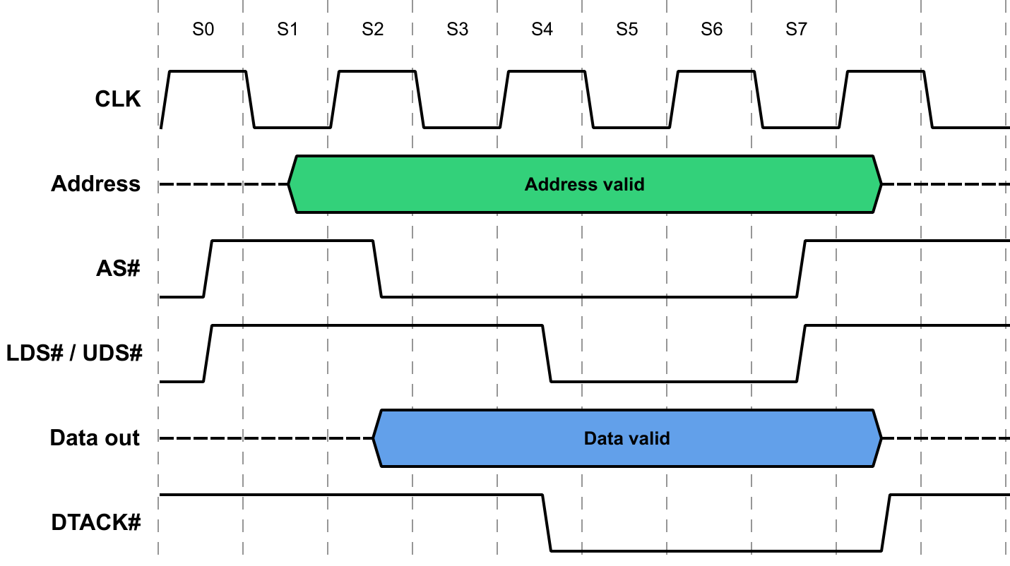
Other unusual things about the bus are the UDS#/LDS# signals (upper and lower data strobe signals). Notice the difference between the read and write diagrams: these are lowered in the write diagram after S4. This means that we don't know which byte of the 16-bit word is written before S6. This becomes an optimization issue in cases where we need that information immediately. It's not a serious issue, but it does cause a delay in such cases (assuming synchronization on the rising edge).
It took me some time to understand the bus based on various versions of the Motorola 68000 datasheet, but I finally managed to get the CPU to read something from the FPGA and later write something to it and read it back!
With the bus interface working, I continued soldering - finally the PCI bus.
Soldering PCI bus signals
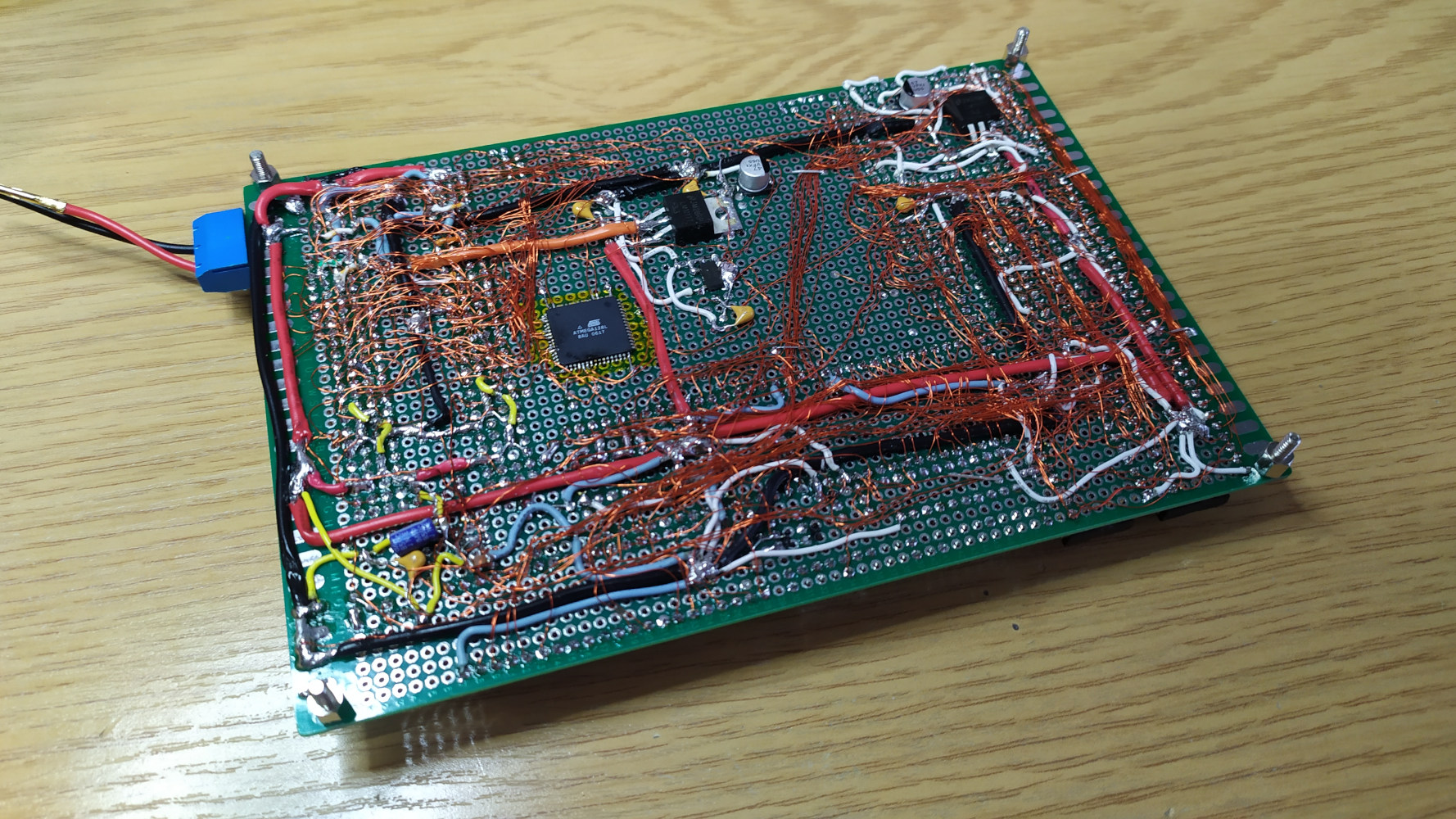
To save on FPGA pins, I used a technique employed by real PCI motherboards: I connected the IDSEL pins of the slots to the AD bus via resistors (75 ohms in my case; typically, it's 100 ohms). Since configuration read/write PCI commands occur on the entire bus, PCI cards need to know which ones are the actual targets of these commands. This information cannot be acquired directly from the address on the AD bus because the address on the bus refers to the data in the configuration space. PCI solves this with an extra IDSEL pin, which is unique for each slot. Boards can implement this pin in two ways. The first method involves dedicated outputs from the PCI bridge, while the second solution uses unused AD pins during these commands. I chose the second solution. It works because configuration commands only define the use of AD pins 0-15 during the address phase. The rest of the pins are unused. The boards and bridges take advantage of this by connecting the AD16-31 pins to the IDSEL pins. During normal operation (memory or I/O reads/writes), this is not a problem because the cards only sample IDSEL when configuration commands occur. The only issue is signal degradation due to extra load on the line. This is solved by adding a resistor and delaying the address phase. With the resistor trick, when the bus runs at 33 MHz, the address is presented on the AD bus for a few cycles before the FRAME# signal finally goes low, giving the IDSEL time to propagate.
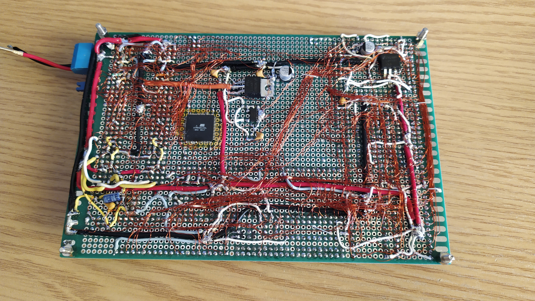
This was also the point where I decided to add an ATmega128 to the board. Its sole purpose in this project is to load the configuration bitstream into the FPGA - it doesn't even manage the system reset. Originally, I wanted the onboard 68000 to handle the FPGA configuration to save on parts. My first thought was to use the MC68681P DUART's output port to load the data in serial mode, as that would easily fit within the available pin count. However, doing the math made me realize that bit-banging a 96 KB bitstream through the DUART with a Motorola 68000 running at just 10 MHz would take entirely too long (probably more than few seconds). I couldn't switch to a faster parallel loading mode either, because that requires at least 9 pins (an 8-bit data bus plus a clock signal) and the DUART only has exactly 8 output pins available. In the end, the most practical way to get the FPGA up and running quickly was to dedicate an ATmega to this one specific task. Adding the ATmega was incredibly straightforward - I only had to provide power, expose the programming pins and wire it to the FPGA configuration pins. I didn't even need to include an external crystal, as the chip runs perfectly on its internal 8 MHz oscillator. On the software side, I was able to reuse the loading code directly from the M8SBC-486 project, since that design uses the exact same microcontroller to bring up a Spartan 2 FPGA. By using the ATmega's hardware SPI Interface, the entire bitstream loads in just a few hundred milliseconds.
First PCI tests
Once I was finally done with the soldering, I could move on to what I’d been waiting for all along: designing the PCI interface logic.
The very first thing I wanted to achieve was doing basic configuration reads off the PCI bus. As I explained in the PCI introduction, the bus is divided into three spaces: memory, I/O and configuration. The Motorola 68000, however, only understands a single unified memory space. To bridge this gap and correctly translate the spaces, I came up with the following memory map design: the first 64 KB of the CPU memory space assigned to the PCI is translated into I/O cycles and mapped to the beginning of the PCI I/O space. This means a CPU memory access at 0x800000 translates directly into a PCI I/O access at 0x0000. The address space above that is passed through as is, so a CPU memory access at 0x900000 becomes a standard PCI memory access at 0x900000. That leaves the configuration space. For this, I decided to borrow the classic mechanism used in standard PCs - accessing it via two registers (which on a PC are two 32-bit I/O ports). The first is the "CONFIG_ADDRESS" register, which I mapped at 0xFFFF00. This is a read/write register that specifies which device on the bus is being addressed and the specific offset within its configuration space. I reused the standard PC structure, which looks like this:
| Bit 31 | Bits 30-24 | Bits 23-16 | Bits 15-11 | Bits 10-8 | Bits 7-0 |
|---|---|---|---|---|---|
| Enable Bit | Reserved | Bus Number | Device Number | Function Number | Register Offset |
(source: OSDev.org - PCI)
I did alter this structure slightly for my system by removing the Enable Bit and Bus Number entries.
So, after writing to the CONFIG_ADDRESS register, the bridge knows exactly what device and offset I want to target. To actually begin the transaction and read or write the data, I then access the "CONFIG_DATA" register. In my design, this is treated as a 32-bit register mapped right next to the address register at 0xFFFF04. The catch here is how it interacts with the 68000's physical 16-bit data bus. Doing a 32-bit read or write in C code forces the CPU to execute two consecutive 16-bit bus cycles. Instead of implementing complex read/write merging inside the FPGA (where it would hold the first 16-bit access and wait to merge it into a single 32-bit PCI transaction) I kept it simple. Every 68000 bus cycle triggers its own distinct PCI access. By properly driving the byte enable lines on the PCI bus, I simply execute them as 8-bit or 16-bit transfers. Finally, to handle the big-endian to little-endian conversion, I chose the value preserving method over address preserving. I cross-wired the data buses internally within the FPGA so that a 32-bit access in the 68000 code correctly translates the bytes around. This ensures that a 32-bit value on the PCI card appears exactly as it would in a system with the same endianness.
While I'm talking about registers, I might as well mention the last one I decided to implement: the "CONFIG_MISC" register. Its address is 0xFFFF08 and it is 16 bits in size. I created it as a way to configure other potential functions of the bridge. The first thing I implemented in this register was the PCI reset line control. I chose to have the FPGA start with the PCI reset active. Once the software is ready to configure the PCI and use it, that first bit in this register is cleared, releasing the reset. This bit is set to 1 when the bitstream is loaded or during a global system reset. I added more features to this register later on, which I will discuss later.
After a few hours of writing VHDL and C code and fixing bugs, I managed to get the PCI configuration reads working! Everything worked fine; no bits were swapped, so I knew that I hadn't made any mistakes when soldering ~40 PCI signals and that there were no signalling issues.
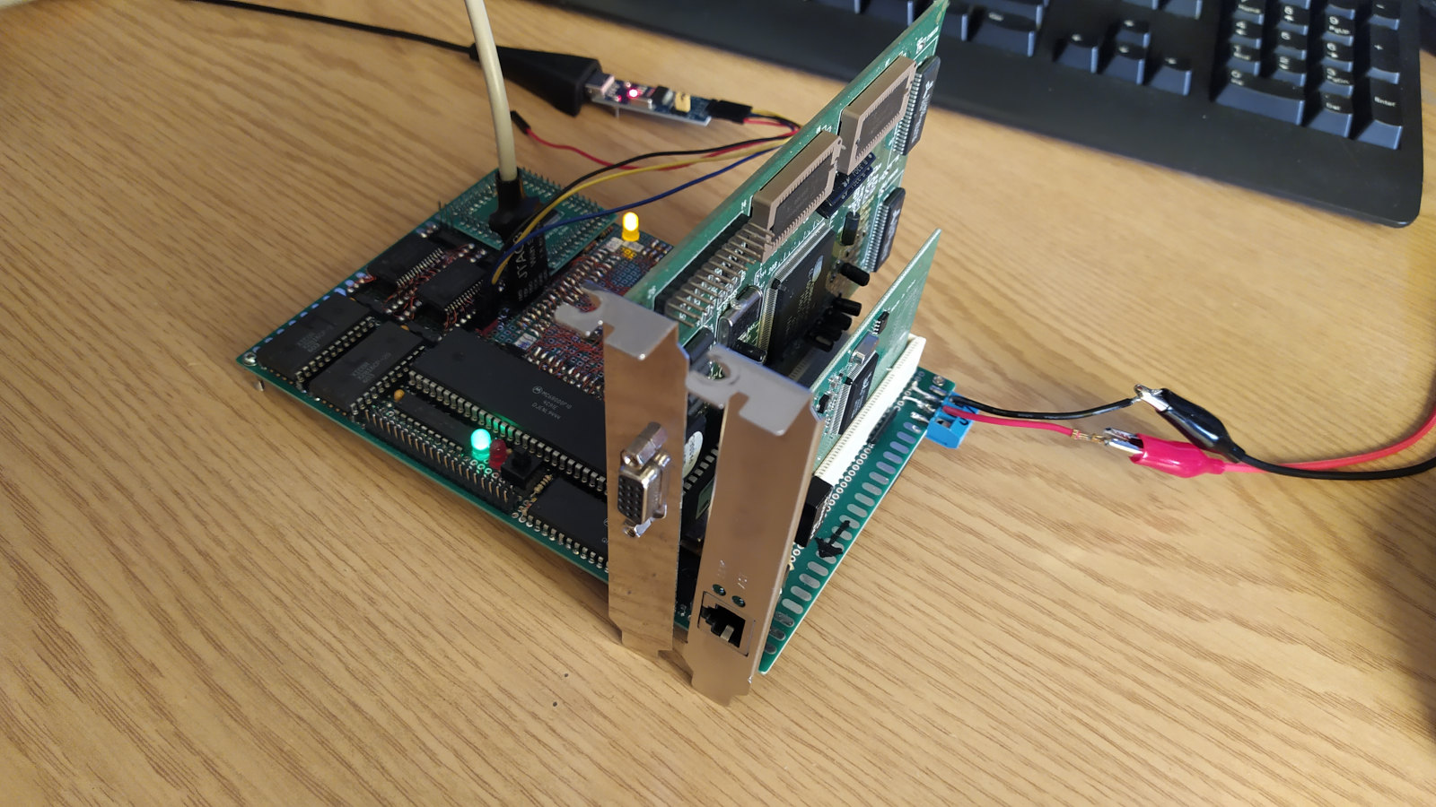
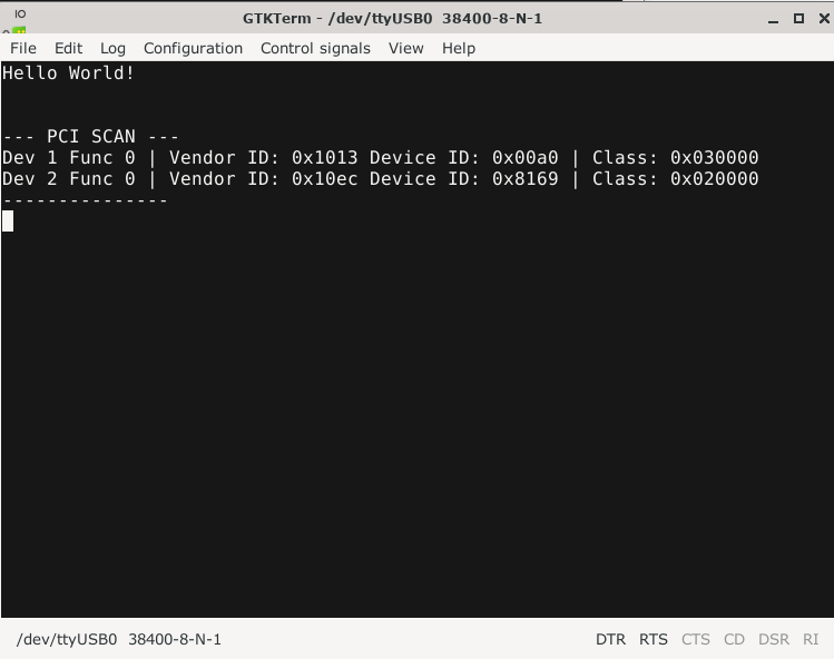
The two first cards I plugged it in the above photo were: Cirrus Logic GD5440 graphics card and Realtek RTL8169 network card. I could see them on the bus, but I couldn't do anything else yet. I started testing various PCI cards from my collection to see if they would show up. Many of them did (network cards, PCI graphics cards, audio cards, etc.), which made me happy! Even one of my PCI-X cards showed up successfully (an Intel gigabit optic fiber network card - imagine a Motorola 68000 using optical fiber ha!). However, I found that some cards were not detected at all and some even caused my bench PSU, which I was using to power everything to shut power off due to an overcurrent situation. After taking a quick look at the schematic, I realized that I had forgotten to pull up the unused GNT# pin. This pin is used when the card does a DMA and drives the bus. The cards probably attempted to drive the bus by misreading this floating signal, which caused a short on the bus and increased the current. Thankfully, because I was using a bench PSU, I didn't fry anything. After fixing this mistake, the non-working cards started working fine. It was fun to just put in a PCI card and see it being recognized by the homebrew with the Motorola 68000 CPU. Ultimately, I started working on the next features so the cards could do more.
Once I successfully got configuration writes working, I could finally probe the devices Base Address Registers (BARs). To figure out how much memory or I/O space a card needs, you write all ones (0xFFFFFFFF) to the targeted BAR, read the value back, invert all the bits and add one. This works because PCI devices hardwire a certain number of their lower address bits to zero to indicate their size requirements. For example, if you write 0xFFFFFFFF to a BAR and read back 0xFFFFFF00, you know the device requires 256 bytes of space (because inverting those bits and adding 1 gives you 0x100 in hex, which is 256). Those hardwired zeros must be sequential starting from the LSB, meaning a PCI card size request is always a power of two. The upper bits (the ones that are actually writable) are then used by the host system to assign the base memory or I/O address where the card will reside. The structure of the register also dictates the absolute minimum size a card can request. For memory spaces, the lowest 4 bits are reserved for extra flags (like the memory type and prefetchable status), which forces the minimum memory allocation to be 16 bytes. For I/O spaces, the lowest 2 bits are reserved (primarily to flag the BAR as an I/O space), meaning the minimum I/O allocation is 4 bytes. Below is an extended version of the previous PCI scan, this time with BAR printing. For this test, I plugged in the Moschip NM9835 PCI serial card and again the GD5440 graphics card.
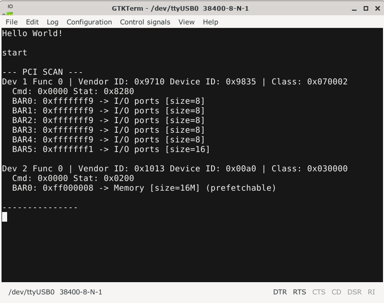
With configuration writes working, I could finally start allocating resources to the cards. I still needed to implement memory and I/O access to actually interface the cards. This was less difficult because I could reuse most of the VHDL logic for both spaces. The main difference lay in the address phase. For memory accesses, the address passed through unmodified, but for I/O accesses, I had to apply the translation (mapping the 0x800000-0x80FFFF CPU memory range down to the 0x0000-0xFFFF PCI I/O range). There was also an quirk with I/O addressing: while PCI memory accesses are always aligned to a double word boundary and rely strictly on byte enables, the legacy I/O architecture requires the lowest address bits to be properly driven: AD0 and AD1, because legacy x86 I/O ports can be packed next to each other within the same double word and PCI cards need these bits to differentiate between exact addresses. That's, because some devices can claim transactions without a BAR being assigned (e.g. "legacy" VGA cards), so the 4-byte alignment rule doesn't always apply. I handled this by decoding AD0 and AD1 using the 68000's A1 address line, combined with the LDS# and UDS# signals.
As with the configuration space, I kept things simple: memory and I/O accesses max out at 16 bits. There is no 32-bit merging: every CPU transaction triggers its own PCI transaction. My PCI state machine starts during the 68000's S6 bus cycle state. By this point, all the information about the CPU's read or write (address, data and UDS# / LDS#) is known, so the FPGA immediately drives the address bus and asserts FRAME#. The FPGA properly supports the target's TRDY# signal while IRDY# is asserted instantly, since the FPGA itself never needs to inject wait states. Each transaction consists of a single data phase since I did not implement burst support. I also added timeout support (master aborts), meaning that if DEVSEL# does not go low within a few clock cycles, the bridge will safely return all ones. Target aborts and retries aren't supported either, so the bridge simply returns all ones in those cases. Making the core PCI logic took me about two days.
My approach to endianness for these spaces was different to that for the configuration registers. Here, I used an "address preserving" translation, meaning the byte addresses match one to one between the CPU and the PCI bus. As the 68000 is big-endian and the PCI bus is little-endian, this setup requires the software to manually swap bytes when writing to 16-bit or 32-bit hardware registers. This method has one major advantage: 8-bit sequential data, like text strings or frame buffer pixel arrays is stored in memory in perfectly continuous order.
For the initial tests, I considered using my experimental PCI FPGA card, but the additional step of uploading the bitstream to the FPGA via JTAG with every power reset made me switch to something else. I instead decided to use the Moschip NM9835 PCI serial card. The datasheet specifies the chip on it as "PCI + Dual UART and 1284 Printer Port" - my card has only two serial ports and an empty printer port header. Another notable feature is that it is 16C550 UART compatible, making programming straightforward. According to its datasheet, the first BAR register corresponds to the first UART port (which is an I/O type BAR). This can actually be seen in the previous screenshot. Writing the driver was pretty straightforward. The logic works like this: If the card is detected during the PCI scan, the first BAR is set to a certain location. I chose the standard PC location of 0x3F8. Then, the card is enabled in the PCI configuration register (I/O accesses are enabled via a bit). Finally, the usual 16C550 initialization code is used (with the 16C550 mapped at 0x8003F8 from the perspective of a Motorola 68000). After that, the serial port is ready.
I had one problem with the serial port: I didn't get any output, even though the code was correct. I remembered that serial ports require -12V and +12V and I confirmed this when I saw that the card used the standard GD75232 serial driver, which requires these voltages. To avoid complicating the board with extra power inputs, I found an interesting module that I bought from AliExpress some time ago in my storage: a tiny step-up buck module that generates 12V and -12V from a single power rail with a maximum current of about 100 mA. This is enough for this job. I quickly soldered it onto the board and finally, I saw the first characters in the serial console connected to the PCI serial card. The first PCI device is working on this homebrew computer!
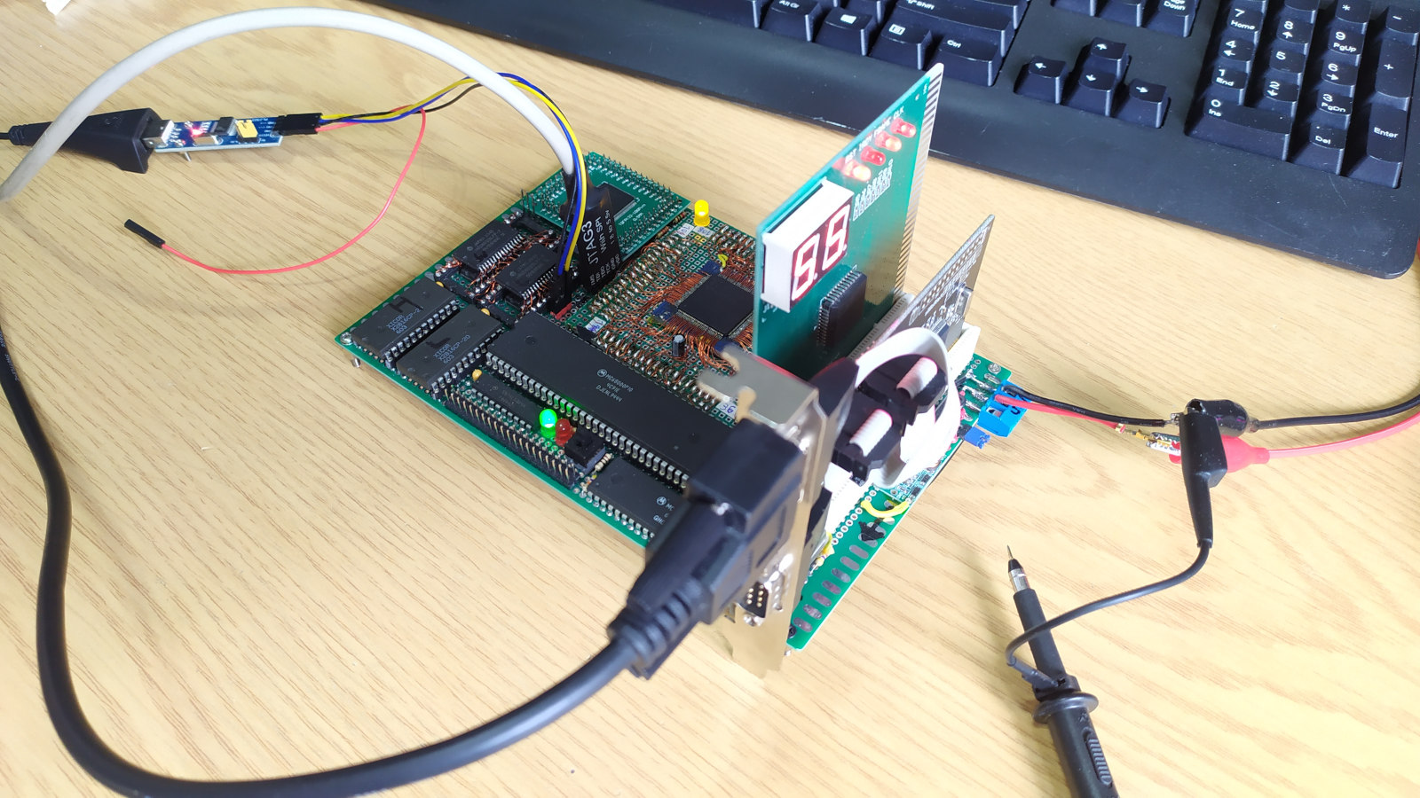
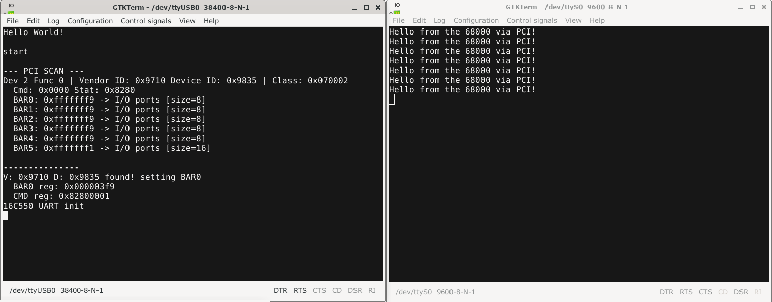
The left is the MC68681P DUART serial terminal and the right is the PCI serial card terminal. Initially, I suspected my implementation of PCI transfers, so that's why I was using a POST card as well. I can confirm that these work fine with this homebrew computer! Device count is from 1 because I reserved 0 to "host bridge", which I planned to add later.
Interrupts
From the moment I introduced interrupts to this project, I knew I wanted the PCI cards to trigger CPU interrupts. Since the PCI serial card can generate simple and easy to handle interrupts (like firing when data is received), it was the perfect test device. To get started, I had to physically wire the interrupt lines. The beauty of this setup is that I could completely bypass the FPGA bridge - it doesn't need to know anything about interrupts at all. PCI INTx# pins are open drain (often referred to as open collector), level triggered (active low) and are designed to be shared. While standard PC motherboards usually dedicate 4 system interrupts to PCI slots, I decided to simplify things and use just two. I wired all 4 interrupt lines (INTA# through INTD#) on a single slot together and connected them to one system interrupt line. This means every function on a given PCI card shares the exact same interrupt, with each physical slot having its own dedicated system interrupt. Since the lines are open drain, I tied them high with pull-up resistors and updated the CPLD's VHDL logic to handle the incoming signals.
I also wanted the ability to mask these signals in software, so I added an interrupt gating feature through my custom CONFIG_MISC register. I mapped the second bit of this register to a physical output pin that connects to a "PCI_GATE" signal on the CPLD. This allows the CPU to fully enable or disable PCI interrupts. With the hardware in place, the software side was straightforward. I configured the card's 16C550 UART to trigger an interrupt whenever it received data and wrote a simple handler to service it. For the initial test, the handler just read the incoming byte (which automatically clears the interrupt on the UART) and echoed it right back out. After uploading the new code to the computer and seeing successful PCI initialization, I typed a character into the terminal connected to the PCI card and immediately saw the data echo back to the screen. It worked perfectly - all driven by hardware interrupts!
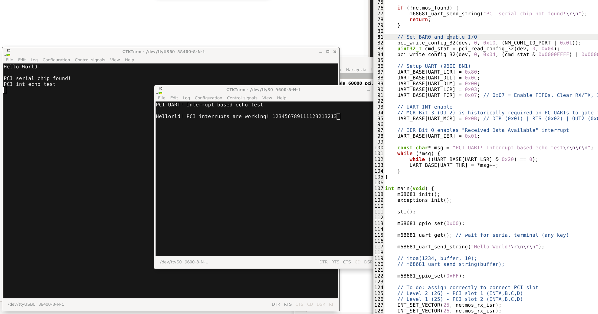
Going further - supporting more cards
At this point, I assumed the system was pretty much done. There was an IDE interface that I didn't solder, but I decided to abandon the idea. This left two 74245s, one 74244, one IDE connector and one LED unused. That's because I became more interested in the PCI and the serial bootloader was just fine for me. At the beginning of this project, I had an idea to make the system try to load the program from the IDE if the serial upload times out. Maybe one day I'll finish it...
Graphics cards
My next goal was to initialize a VGA graphics card! The tricky part with PCI VGA cards is that they usually rely on their onboard Video BIOS (VBIOS) to initialize them into standard VGA mode. Once in that mode, they expose the legacy VGA registers and can be controlled directly (similar to programming VGA in protected mode without using the well known int 10h BIOS calls). The issue? These VBIOS ROMs are entirely x86 assembly. I couldn't run them on a Motorola 68000 without writing a bulky x86 emulator. Instead, I decided to try initializing a VGA card entirely from scratch. Digging through my parts bin, I found the perfect candidate: a Cirrus Logic GD5440. These chips are incredibly well documented and frequently emulated (like QEMU's cirrus-vga). I discovered that their "unlocking sequence" (which forces the card into legacy VGA mode) is just a couple of I/O writes. In this mode, the card doesn't even need a BAR assignment; it acts as a legacy device living at fixed PC I/O and memory addresses. All it requires is enabling the I/O and memory access bits in its PCI configuration command register.
I had just one slight issue: legacy VGA requires memory addresses below 1 MB (specifically the 0xA0000-0xBFFFF area). While my I/O was already translated properly, memory was not. My bridge mapped CPU memory accesses at 0x810000-0xFFFFFF to the exact same addresses on the PCI bus. To fix this, I added a "legacy memory translation" bit (bit 3) to my CONFIG_MISC register. When enabled, it translates CPU accesses in the 0x810000-0x8FFFFF range down to 0x010000-0x0FFFFF on the PCI bus. This gave me seamless access to the sub-1MB video memory just by flipping a single bit. The rest of the memory (0x900000-0xFFFFFF) remains mapped one to one when this bit is enabled.
The GD544x unlock is relatively simple:
3C4h index  6  (R/W):  Unlock ALL Extensions
bit  0-2,4  Writing 12h to this register enables extensions.
            Read back 0Fh if locked.
            Bits 3,5-7 are ignored on write.
(Source: GitHub - whatisaphone/tower-pc - CIRRUS.TXT)
So the unlocking comes down to two simple I/O writes:
pci_outb(0x3C4, 0x06);
pci_outb(0x3C5, 0x12);
(This actually applies to some other Cirrus Logic cards as well!)
After sending that sequence, a standard VGA initialization routine can be used to put the card into text mode (resetting the sequencer, configuring the miscellaneous output register, programming the standard VGA register blocks, setting up the DAC and uploading the font). This Cirrus Logic card is great because, unlike other cards I had in storage (like the ATI Mach64 or Matrox) it doesn't require a highly complex register setup to manually adjust clock frequencies or DRAM timings. Since standard VGA setup mostly relies on I/O port operations, I used AI again to quickly generate the C code for the initialization sequence. After putting it all together and uploading the new code, I finally saw "Hello World!" printed on the monitor! Card was initialized in the standard 80x25, 16-color VGA text mode (known as mode 03h).
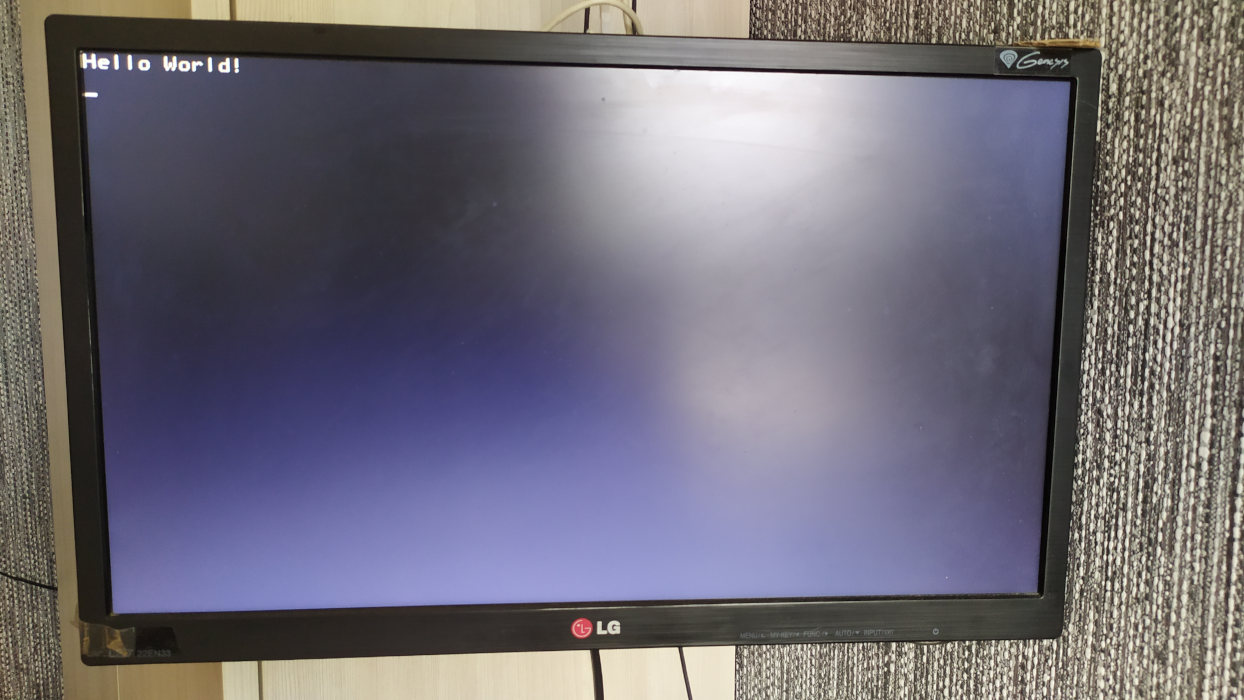
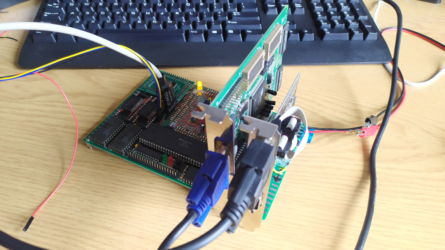
Other tasks, like moving the hardware cursor, involved standard VGA I/O code exactly the kind you would see in an x86 protected mode OSDev tutorial. In fact, I suspect a lot of standard PC code could actually be ported directly to this machine. The only major thing you have to keep in mind is the endianness.
While 8-bit accesses write sequentially exactly as expected, 16-bit accesses are a different story. I ran right into this while writing a standard character and attribute macro for the 80x25 text mode. In this mode, one character block on the screen takes up exactly two bytes in video memory. The first byte is the actual ASCII character and the second byte is its attribute (which defines the foreground and background colors and optionally controls blinking). These are stored sequentially, so the byte at 0xB8000 is the character and 0xB8001 is the attribute. In a typical x86 operating system environment, there's a popular macro to set both of these at once:
#define VGA_ENTRY(ch, attr) ((uint16_t)(ch) | ((uint16_t)(attr) << 8))
Using a uint16_t pointer allows the CPU to do a single 16-bit write instead of two separate 8-bit writes, which is a great little optimization. Since my FPGA bridge fully supports 16-bit writes, I figured, why not use it? However, because my bridge uses "address preserving" translation, it doesn't automatically byte swap 16-bit data. When you use that macro, the big-endian Motorola 68000 writes the most significant byte of the 16-bit word to the lower address. This means the little-endian VGA card receives the attribute as the character and the character as the attribute! When I first used the standard x86 macro I just ended up with a screen full of colorful garbage. I just had to swap the shift logic to pack the data in reverse order:
#define VGA_ENTRY(ch, attr) ((uint16_t)(attr) | ((uint16_t)(ch) << 8)) // reverse order
Later on, I also got the card to initialize in 320x200 256-color graphics mode (mode 13h). The performance of my bridge was not bad; the entire screen was filled in about 300 milliseconds (the framebuffer size in this mode is 64000 bytes, so the throughput is about 200 KB/s - this is only an estimate from screen recording; I could have written test code for this, but I didn't). Below is a video of the GD5440 graphics and serial cards connected and working simultaneously.
At this point, I also rewrote the entire source code. I moved all peripheral initialization code to its own files. I expanded the PCI scan to store information about PCI cards and when a card is detected, it tries to load the corresponding driver (drivers are registered before the PCI scan and have their own dedicated source files). I upgraded the interrupt logic to allow for shared interrupts. Drivers are passed information about the PCI card, including its interrupt line, from the PCI scan function. With this, the driver can request that the new interrupt subsystem hook up to the interrupt. One interrupt can have multiple handlers. I also split the VGA code into card specific initialization and general VGA initialization. The card specific code hooks up as a driver for the card and at the end, calls the VGA init code. I recommend visiting the GitHub repository for this project to see how the code is organized. The main file is under 100 lines!
With the help of an internet search, experimentation, reverse engineering VBIOSes and AI, I also got two more VGA cards to work:
- S3 Trio64V2/DX (S3 86C775): I found the initialization sequence for this card via AI on the internet. It involved a few I/O writes, similar to the GD5440. I wrote a separate driver with a different initialization code and it fully works!
- IGS IGA 1680_A: This is an obscure PCI graphics card. I got it from a friend a long time ago and there isn't much information about it on the internet. I disassembled its VBIOS and after some trial and error, I found two I/O writes that made it display something. I had trouble getting the color to work. The card seemed to initialize in grayscale mode. After looking at the disassembly again, I spotted one more I/O write. This made the card work fine in 80x25, 16-color text mode. However, an issue appeared in the 320x200 graphics mode with this I/O write. The addressing seemed broken (the screen was squished and repeated, which was strange). I experimented and dug further, but I didn't get far. I gave up on getting this one to work fully, but I still consider it a success because it's the third card that works and actually displays something!
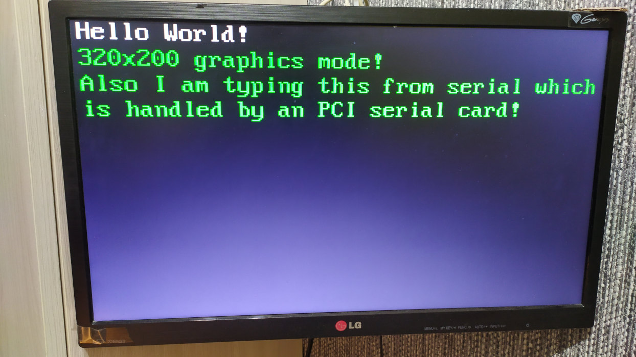
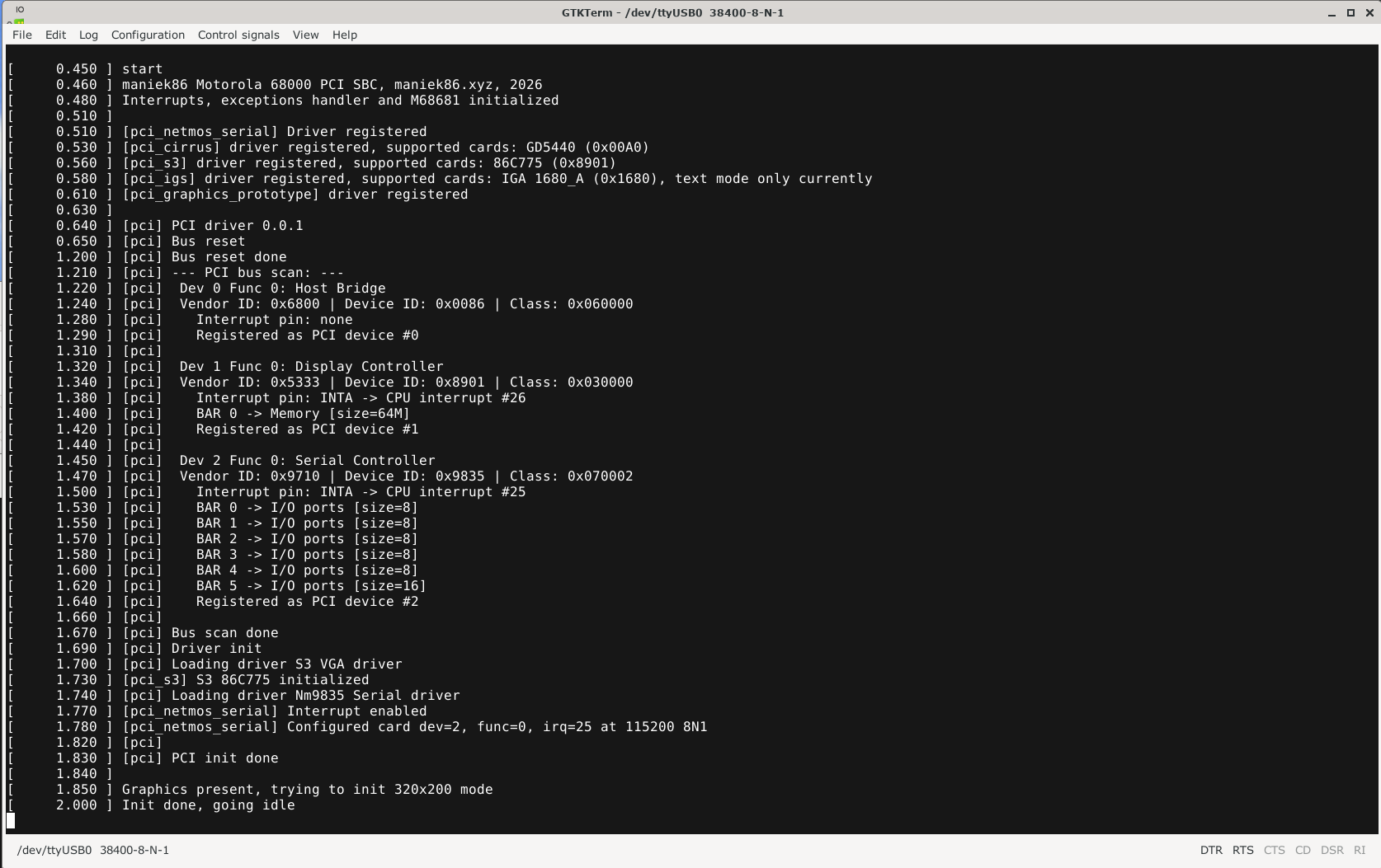
In the end, I updated the VHDL code one last time to add a dummy PCI device - the host bridge. This made the FPGA PCI bridge appear more complete. However, I didn't implement extra features such as bus error reporting via PCI status bits. Below is a screenshot from the late firmware console output.
Networking
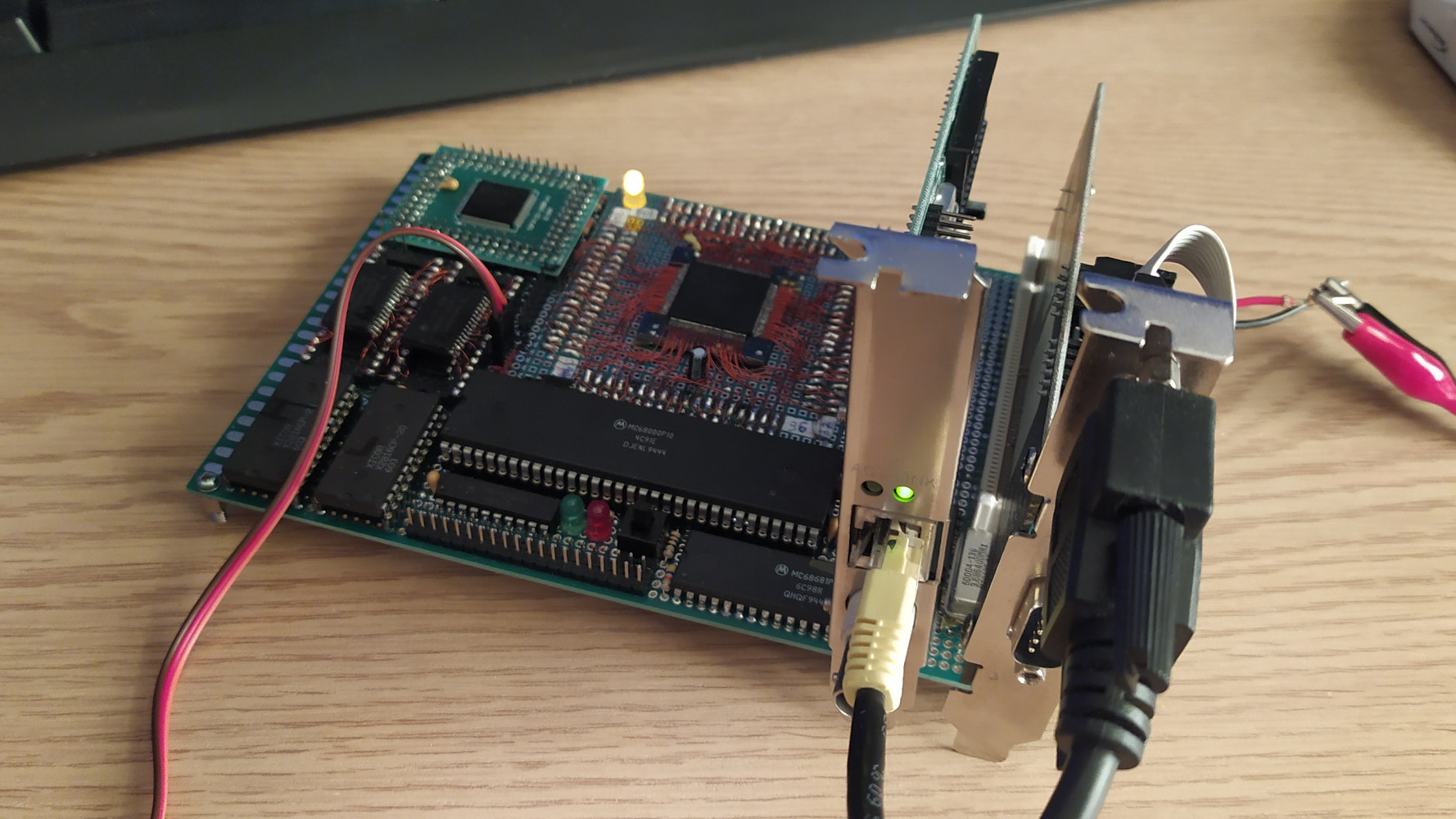
The last thing I wanted to try was a networking card that I found in my storage: an RTL8029. It's a PCI NIC chip. What makes it special is that it doesn't require DMA to operate. In my design, I omitted DMA mainly because I ran out of pins on the Spartan 2 FPGA. Other PCI network cards, such as the popular RTL8139 rely on DMA. Even the Intel PCI-X optic fiber card that I got to detect in this computer requires DMA. Programming the RTL8029 is simple because it's basically NE2000 compatible card but with a PCI bus. I just have to assign the I/O BAR and enable I/O accesses, like with the serial card and it's ready to go.
Since I had almost finished the project (the previous card taught me a lot about the PCI bus), I decided to take a shortcut. This time, I used an AI agent to write the entire driver and simple network stack for me. I justify this because I just wanted to see how it could work as a proof of concept. After studying PCI, soldering this homebrew and writing VHDL, I was exhausted and just wanted to see what was possible with this homebrew. I'm leaving in-depth networking learning for the future. After a few minutes of the AI working and me correcting its mistakes (it hooked up the interrupts incorrectly), I uploaded the code and it actually worked! It implemented a simple networking stack, an RTL8029 driver, a Telnet command control server and a simple HTTP server. All of this was processed on a Motorola 68000 homebrew computer with a PCI bus! The source code is also available in the repository.
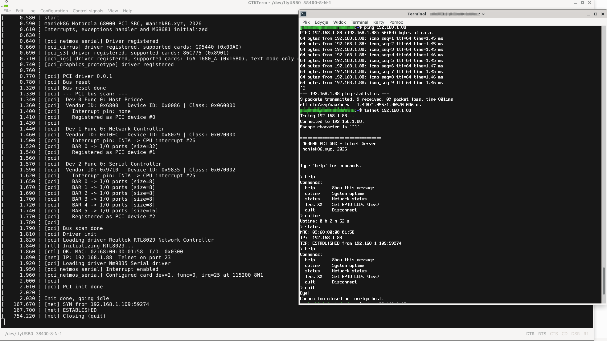
Sumarry
The RTL8029 network card was the last piece of hardware I tested before sitting down to write this article. Even with the current limitation of no DMA support, the possibilities are practically endless - it really just comes down to writing the drivers, because the PCI subsystem works perfectly. I originally built this computer with the goal of learning the low level mechanics of the PCI bus from the bridge's perspective, laying the groundwork for some even more ambitious projects I have planned for the future.
To keep this article readable, I had to omit a lot of deep technical details, so I’ve decided to open-source and share all the project files. Whether you want to dive into the architecture, learn how the bus translation works or just borrow snippets of my VHDL for your own builds, feel free to use it. I actually believe this might be the first homebrew computer with a fully functional PCI bus built entirely on a prototype board! The PCI standard is amazing: because there are thousands of cheap, varied cards out there, a bus like this lets you add virtually any interface to a custom computer. If you are still reading this - thank you for sticking with me until the end!
Finally, a massive special thanks to Shadowdestroyer777 for sending me the scrap hardware that made this possible, including the Motorola 68000 processor used in this project and the scrappy motherboards from which I desoldered the actual PCI slots.
Potential questions
- Which cards require DMA (Bus Mastering) and therefore won't work on this computer?
Because I didn't implement PCI bus mastering (DMA) in the FPGA, the 68000 CPU has to manually handle every single byte of data transferred across the bus. Cards that strictly require DMA to function simply won't work here. This includes higher end 3D graphics cards or accelerators, most PCI sound cards (which rely on DMA to feed continuous audio buffers), USB controller cards, TV capture cards, SCSI controllers, many network cards and probably more. - What other cards could also work on this system?
Anything that can operate using standard memory mapped I/O or legacy port I/O (PIO) without needing to take control of the bus. PCI IDE controller cards are a great example, as they can usually fall back to PIO mode. - What about PCI bridges?
I omitted support for these to keep the design simple. Currently when I plug in a bridge card, it shows up in my PCI scan just fine. In order to access the devices located behind the bridge, a few additional features would need to be implemented. I suspect this wouldn't be too challenging: the FPGA would require an update to generate Type 1 configuration cycles and the software would require some extra code to handle the enumeration of the secondary buses.